Transport Function Analysis of Thermoelectric Properties
The quantum mechanical description of transport, including thermal and electrical transport, is typically derived using the Boltzmann Transport Equation. This utilizes an equilibrium distribution function (e.g. the Fermi-Dirac distribution function for electron transport) and an average relaxation time for a given particle to return to the equilibrium when displaced by a driving force. The Boltzmann Transport Equation can describe both classical and quantum system and ideal for interpreting the effective parameters used in the common semi-classical description. The Landauer Approach [1] devised for quantum sized systems and the more general Green-Kubo relations give essentially the same result.
Complex Fermi Surfaces
The Boltzmann Transport Equation enables the description of electron transport in a materials with a complex band structure. This is important for thermoelectrics because the Fermi Surface of conducting electrons typically contains many separate pockets, large anisotropy and/or unusual (non ellipsoidal) shapes. Keep in mind that electrical conductivity \(\sigma_{ij}\), Seebeck Coefficient \(\alpha_{ij}\) or \(S_{ij}\), and thermal conductivity \(\kappa_{ij}\) are symmetric second rank tensor properties, in that they describe the vector flux (e.g. current density) that results from a vector force (e.g. electric field).
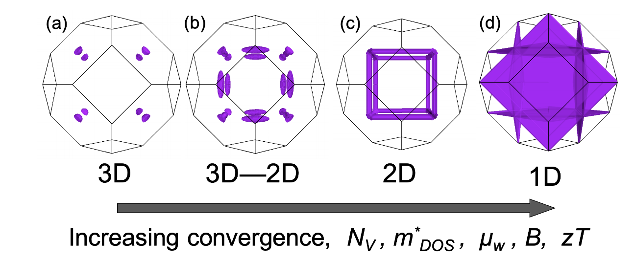
The Fermi Surfaces in Lead Chalcogenides, such as PbTe, can have exceptionally high effective valley degeneracy due to band convergence [23].
While a free electron Fermi surface from \(E=\frac{\hbar^2k^2}{2m}\) is a single sphere centered at Γ the Fermi surfaces of real semiconductors are much more complex and this affects their properties. A single band typically makes an ellipsoidal Fermi surface. If the band extremum is not at Γ (\(k=0\)) there will be multiple symmetrically equivalent Fermi surface pockets leading to Valley Degeneracy \(N_\text{V}\). Two different bands may have similar energy giving higher effective valley degeneracy due to band convergence. Multiple bands at the same band extremum will lead to orbital degeneracy and warped Fermi surfaces that can not be described by an ellipse with tensorial effective mass. The joining of Fermi surfaces into tubes or sheets enables a density-of-states that resembles 2-dimensional or 1-dimensional systems and leads to higher effective valley degeneracy [20, 21, 23] or Fermi surface complexity factor [22].
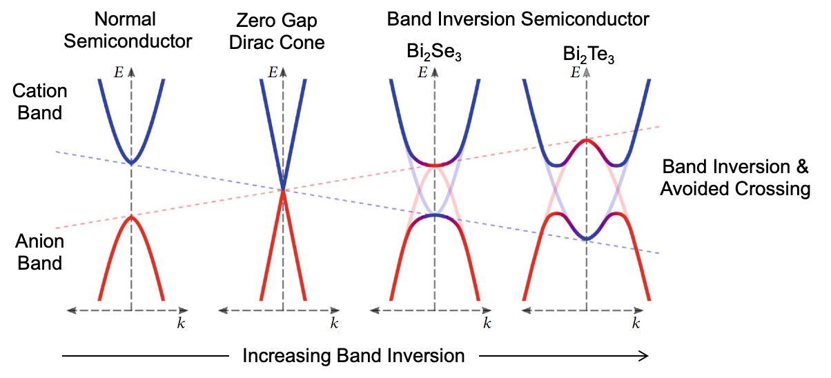
The Fermi Surfaces in Bi₂Te₃-type thermoelectrics, have high effective valley degeneracy due to band inversion and warping [24, 25].
Band inversion, such as that which leads to band structures with unusual topologies also can lead to warped Fermi surfaces with high valley degeneracy as found in Bi₂Te₃-type thermoelectrics [24, 25].
Boltzmann Transport Equation
The Boltzmann Transport Equation form of the thermoelectric transport properties can be described using the same Transport Function \(\sigma_{E}\) [1, 2, 3].
$$\sigma= \int{\sigma_{E}\frac{-df}{dE}dE}$$
$$\alpha= \frac{1}{\sigma (-e)T} \int{\sigma_{E}(E-E_F)\frac{-df}{dE}dE}$$
$$\kappa_e= \frac{1}{e^2 T^2} \int{\sigma_{E}(E-E_F)^2\frac{-df}{dE}dE}-T\alpha^2 \sigma$$
where \(f\) is the Fermi-Dirac distribution function, \(E_{F}\) is the Fermi Level and \(\kappa_e\) is the electronic contribution to the thermal conductivity. Here the \((-e)\) ensures that electrons with charge \((-e)\) above the Fermi level (\(E > E_F)\) will contribute \(\alpha < 0\). Electrons below the Fermi level (\(E < E_F)\) will contribute \(\alpha > 0\) but are not considered holes. In the semiconductor physics terminology used for semi-classical models "electrons" counted for \(n_e\) must reside in a conduction band while "holes" counted for \(n_h\) are the absence of electrons that reside in a valence band. A reformulation of the transport integrals for holes can be used later but not usually done for DFT based electronic structures.
Transport function
The transport function \({\sigma_E}_{ij}(E)\) is a second rank tensor sum of velocities \(v_i = \frac{dE}{\hbar dk_i}\) and relaxation time \(\tau\) over the surface \(A\) of constant energy \(E\).
$${\sigma_E}_{ij}(E) = \frac{e^2}{4\pi^3}\oint_E v_i v_j \tau \frac{dA}{\nabla_k E}$$
recognizing that the density of electronic states \(g(E) = \frac{1}{4\pi^3}\frac{dA}{\nabla_k E}\) one sees that for an isotropic band structure
$$\sigma_E \sim \frac{2e^2}{3}v^2 \tau g$$
Seebeck Formulas
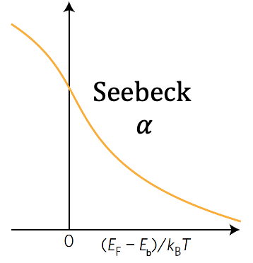
We like to think of the Seebeck coefficient as primarily a measure of the Fermi Level, relative to the band edge. This can be seen in the common, simplified forms of the Seebeck coefficient [3].
Metals
For metals which have the Fermi Level deep within a band, the Mott Equation is often used:
$$\alpha = \frac{\pi^2}{3}\frac{k_{B}^2T}{q}\frac{d\sigma_E}{\sigma_EdE}$$When the band is parabolic and simple phonon scattering dominates, the Mott Equation simplifies to:
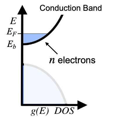
$$\alpha = \frac{8\pi^2k_{B}^2}{3qh^2}m^* T\left(\frac{\pi}{3n}\right)^{2/3}=\frac{\pi^2}{3}\frac{k_{B}^2}{q}\frac{T}{E_F}$$where \(m^*\) is the density of states effective mass (or replace with \(m^*(1+\lambda)\) where \(\lambda\) is the scattering parameter), \(n\) the density of charge carriers (both always positive for electrons and holes) and \(E_F\) is the Fermi Level relative to the band edge \(E_b\). Use \((E_F - E_b)\) in place of \(E_F\) if \(E_b\) is not defined to be zero. Note that \(\alpha < 0\) (n-type) for a conduction band (\(E_F > E_b\) for \(E_F\) to be inside the band) because \(q=-e\) for electrons. When used for a valence band, the electrochemical potential of the holes is typically used for the Fermi Level (\(E_F > E_b\) for \(E_F\) to be inside the valence band) so with \(q=+e\) gives \(\alpha > 0\) (p-type).
Insulators
For intrinsic semiconductor and insulators, where \(E_F\) is in the band gap far from a band edge \(E_b\), the Seebeck coefficient is sometimes approximated as:
$$\alpha = \frac{E_b - E_F}{qT} + A$$
where A is often ignored as if it were a small constant. Again \(\alpha < 0\) (n-type) for electrons \(q=-e\) because \(E_F < E_b\) for non-degenerate semiconductor.
Heikes Formula
The Heikes formula [3, 4] is often used to describe narrow band systems where \(c\) is the fraction of filled states in the narrow band.
$$\alpha = \frac{k_B}{q} \ln\left(\frac{1-c}{c}\right)$$
The conductivity also has a simple form [3]:
$$\sigma = c(1-c) \frac{\int\sigma_{E}dE}{k_B T}$$
Electron Scattering
The quantum mechanical description to determine scattering rate \(1/\tau\) is most easily seen using Fermi's Golden Rule. The scattering rate for a particle with energy \(E\) is
$$1/\tau(k) = n_\text{s} g(E) |\langle k |\hat{H'}| k' \rangle|^2$$
\(n_\text{s}\) is the density of scattering centers. \(\tau(k)\) is the scattering rate of an electron state \(k\) with energy \(E\). \(g(E)\) is the density-of-states that the electron can scatter into. Here \(\langle k |\hat{H'}| k' \rangle\) is meant to represent the average matrix element for the perturbation Hamiltonian \(H'\) including the forward scattering term, in the correct units [5]. Here elastic scattering is assumed, where the energy of the electron is unchanged.
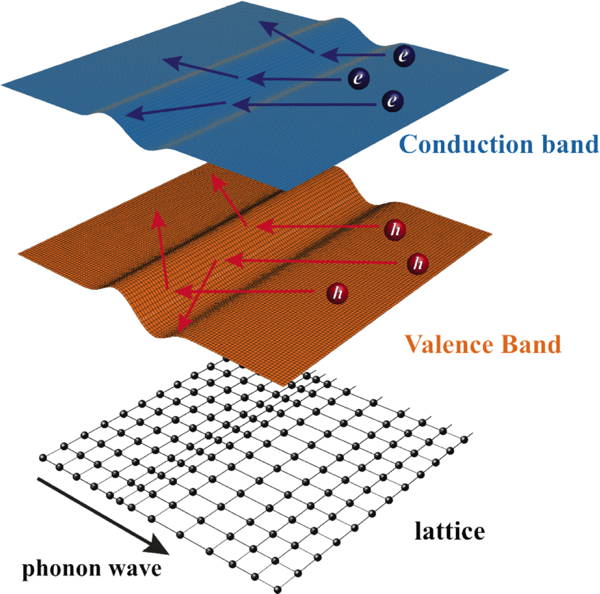
Scattering of electrons by phonons described by a deformation potential [6].
Scattering of Electrons by Phonons
The scattering of electrons by phonons is complex but can now be calculated by DFT methods for specific cases. The most useful approximation to generally describe what phonon scattering is and model experimental properties is based on deformation potential scattering (deformation of the crystal changes the energy of electrons which scatters transporting electrons) [6] where the scattering rate for an electron with energy \(E\) is given by [7]:
$$1/\tau = \frac{\sqrt{2} }{\pi \hbar^4 } \frac{\Xi^2(m^*_b )^{3/2} }{C_l} (k_\text{B}T) E^{1/2}$$\(m^*_b\) is the density-of-states effective mass from the density of electron states that the electron can scatter into. \(\Xi\) is the effective deformation potential [5]. This is the change in electron energy due to the deformation of the material, calculated from the matrix element \(\langle k |\hat{H'}| k' \rangle\) which also depends on the elastic constants (here \(C_l\) is an effective elastic constant [6, 7]) as it relates the force and energy required to deform the material.
Although this scattering is often called Acoustic Phonon Scattering, and the above equation is based on such a theory, phonon scattering in complex thermoelectric materials, may actually be dominated by optical phonons. The effective temperature and energy dependence (above the Debye temperature) of the polar and non-polar optical phonon scattering [8], appears to approximate the temperature and energy dependence given above. Non-polar optical-phonon deformation-potential scattering can be shown to have the same analytic form as that given above [6, 7]. For comparison with experimental transport properties the \(\Xi\) parameter above is best considered to be due to the combined effect of acoustic, non-polar optical and polar optical phonons.
When there is no inter-valley scattering, \(m^*_b\) characterizes the DOS of one valley. This leads to:
$$B \sim \frac{N_V}{m^*_I \kappa_L}$$and the strategy that to achieve high thermoelectric quality factor \(B\), and therefore maximum \(zT\) one desires to have a high valley degeneracy \(N_V\) where electrons can not scatter into different valleys [9, 10]. If electrons could scatter as easily into another valley as the one it is already in, there would be no advantage for valley degeneracy. In some cases such as L-L inter-valley scattering in PbTe the inter-valley scattering is forbidden by symmetry making inter-valley scattering a small, higher-order effect. The inter-valley scattering of ∆-line electrons in n-type Si is reduced but non-zero [11]. Good thermoelectric materials [9, 12] tend to have high valley degeneracy from pockets at different k-points in the Brillouin Zone. Having multiple bands at the same k-point, sometimes called orbital degeneracy [10] may not lead to higher \(B\) or \(\mu_w\) because inter-valley scattering may be as strong as intra-valley scattering [14].
The resultant mobility from phonon scattering is typically described with a \(\mu \sim T^{-3/2}\) temperature dependence. This arises from the number of phonons depending on \(k_\text{B} T\) in the equation for \(\tau\) combined with the energy term \(E^{1/2}\). In the non-degenerate semiconductor limit (lightly doped semiconductors) the energy of an electron is proportional to \(k_\text{B} T\) like a classical particle giving \(\mu \sim T^{-3/2}\). While in the degenerate limit (metal or heavily doped semiconductor) the energy of conducting electrons are nearly constant (the Fermi Level) and so the mobility of a metal is \(\mu \sim T^{-1}\) or \(\rho \sim T^{1}\)), consistent with the semi-classical description given for metals and semiconductors .
Grain Boundary Resistance
In thermoelectrics and other complex semiconductors a decreasing resistivity with temperature (in contrast to typical metals and degenerately doped Thermoelectric materials) is observed in many polycrystalline materials due to grain boundary resistance [14, 15]. Many physics texts have perfect, single crystalline materials in mind, and consider only point defects. The scattering mechanism often considered with this temperature dependence is that due to an isolated charged impurity called ionized impurity scattering. Although a charged grain boundary might be considered a 2D array of ionized impurities the material inhomogeneity as well as the trapping of charge carriers leads to fundamentally different phenomena [14]. Polaron hopping charge transport also has a similar temperature dependence to that found in charged grain boundaries, but the mechanisms can be distinguished with the aid of careful thermoelectric measurements [16]
Transport Edge and Transport Exponent
The most useful form of the transport function is a simple power law that begins at a Transport Edge \(E_t\) which is often a band edge \(E_b\) discussed above where the density of states vanishes but it could be due to the mobility vanishing.
$$\begin{array}{lr} {\sigma_E}(T,E) = {\sigma_{E_0}}(T)\left(\frac{E-E_t}{k_B T}\right)^s & (E>E_t) \\ {\sigma_E}(T,E) = 0 & (E < E_t) \end{array}$$
Here \(s\) is the Transport Exponent and depends on the mechanism of charge transport.
The transport function prefactor \(\sigma_{E_0}\) is Temperature but not Energy dependent.
Effective Mass Model
The Effective Mass Model facilitates discussing and comparing the electronic properties of thermoelectric materials by defining the effective parameters (\(m^* \text{ and } \mu_\text{w}\)) that would give the same properties as a simple parabolic band semiconductor: a power law form of the transport function \(\sigma_{E}\) described above with \(s=1\).
The transport function prefactor \(\sigma_{E_0}\) is then related to the weighted mobility \(\mu_\text{w}\) [17] and the Electronic Thermoelectric Quality Factor \(B_E\) [18].
$$ \sigma_{E_0} = \frac{{8\pi e {{\left( {2{m_e}} \right)}^{3/2}}}}{{3{h^3}}} {\left(k_\text{B} T\right)}^{3/2} \mu_w \\ B_E = \frac{k_B^2}{e^2} \sigma_{E_0} \quad \quad B=\frac{B_E T}{\kappa_\text{L}}$$
The weighted mobility is related to the mobility parameter \(\mu_0\) and Seebeck effective mass
$$\mu_\text{w} = \mu_0 \left( \frac{m^*_\text{S}}{m_e} \right)^{3/2}$$
The Seebeck effective mass \(m^*_\text{S}\) (a DOS mass) is derived from measurements of the Seebeck coefficient and charge carrier concentration. This arises from the above equation for weighted mobility and knowledge of \(n\) or measurements of \(n_\text{H}\). Note that the drift mobility and Hall mobility change with doping. In the non-degenerate limit (low \(n\)) the drift mobility is \(\mu_\text{cl} = \frac{4}{3\sqrt{\pi}}\mu_0\) and the Hall mobility is \(\mu_\text{H,0} = \frac{\sqrt{\pi}}{2}\mu_0\) [2,19]
The Hall factor \(r_\text{H}=\frac{n}{n_\text{H}}\) varies from \(r_\text{H,0}=\frac{3\pi}{8}\) in the non-degenerate limit to 1 in the degenerate limit.
The effective mass model in terms of Fermi Integrals
Using the reduced variables relative to the transport edge
$$\eta = \frac{E_\text{F}}{k_\text{B}T} \qquad \varepsilon= \frac{E}{k_\text{B}T}$$
where \(E_\text{F}>0\) for a degenerate semiconductor (metal-like) and \(E_\text{F}<0\) for a non-degenerate semicoductor (intrinsic semiconductor-like) meaning
$$\begin{array}{ccr} \eta = \frac{E_\text{F} -E_\text{t}}{k_\text{B}T} & \varepsilon= \frac{E -E_\text{t}}{k_\text{B}T} & \text{for a conduction band}\\ \eta = \frac{E_\text{t}-E_\text{F}}{k_\text{B}T} & \varepsilon= \frac{E_\text{t}-E}{k_\text{B}T} & \text{for a valence band} \end{array}$$
the Fermi Integrals are
$$F_j=F_j(\eta)=\int_{0}^{\infty}\frac{\varepsilon^j}{1+e^{\varepsilon-\eta}}d\varepsilon$$
The transport functions within the effective mass model (\(s=1\)) is [19]
$$\begin{array}{cc} \sigma = \sigma_{E_0} F_0 & n = 4\pi \frac{\left(2 m^*_\text{S}k_\text{B}T \right)^{3/2}}{h^3} F_{1/2} \\ \alpha = \frac{k_\text{B}}{q}\left(\frac{2F_1}{F_0}-\eta\right) & \mu_\text{H} = \mu_0 \frac{F_{-1/2}}{2F_0} \\ L = \frac{k_\text{B}^2}{e^2}\left(\frac{3F_0F_2-4F_1^2}{F_0^2}\right) & n_\text{H} = n \frac{4F_0^2}{3F_{-1/2}F_{1/2}} \end{array}$$
where \(q=-e\) for a conduction band (electron-like) and \(q=+e\) for a valence band (hole-like). Note that \(\alpha\), \(m^*_\text{S}\) and \(L\) are isotropic for a single band system within this approximation while \(\sigma\), \(\mu_\text{w}\) and \(\mu_\text{H}\) have the 2nd rank tensor anisotropy of \( \sigma_{E_0}\) due to different conductivity mass \(m_\text{I}\) and relaxation time \(\tau\) along the principle directions [22].
Bipolar effects
Bipolar effects, should be expected for non-degenerate or intrinsic semiconductors.
For multiple, noninteracting bands where each band conducts in parallel the overall transport properties are given by a weighted sum of each channel \(i\) [19]:
$$\begin{array}{cc} \sigma = \sum\limits_{i} \sigma_i & \alpha = \frac{1}{\sigma}\sum\limits_{i} \alpha_i \sigma_i \\ \mu_\text{H} = \frac{1}{\sigma}\sum\limits_{i} \mu_\text{H,i} \sigma_i & R_\text{H} = \frac{1}{\sigma^2}\sum\limits_{i} R_\text{H,i} \sigma_i^2 \end{array} \\ \kappa_e = \sum\limits_{i} L_i \sigma_i T + \sum\limits_{i} \alpha_i^2 \sigma_iT - \alpha^2 \sigma T$$
Where here \(\mu_\text{H}\ < 0 \) for electrons and \(\mu_\text{H}\ > 0 \) for holes. Note that the anisotropy of \(\sigma\) makes \(\alpha\) anisotropic even though the \(\alpha_i\) might be isotropic for each band.
References
[1] M. Dylla, S. Kang, G. J. Snyder, E. S. Toberer, et al. "Thermoelectric Transport Theory" Chapter II in A. Zevalkink, S. D. Kang, G. J. Snyder, E. S. Toberer, et al. "A practical field guide to thermoelectrics: Fundamentals, synthesis, and characterization" Applied Physics Reviews 5, 021303 (2018). \(\sigma_{E}=q^2 G(E)\)
[2] S. Kang and G.J. Snyder "Transport property analysis method for thermoelectric materials: material quality factor and the effective mass model" Chapter VI in A. Zevalkink, S. D. Kang, G. J. Snyder, E. S. Toberer, et al. "A practical field guide to thermoelectrics: Fundamentals, synthesis, and characterization" Applied Physics Reviews 5, 021303 (2018)
[3] Stephen D. Kang and G. J. Snyder "Charge-Transport Model for Conducting Polymers" Nature Materials 16, 252 (2017). Common forms of the Seebeck coefficient in the supplemental material.
[4] Heikes and Ure "Thermoelectricity: Science and Engineering" Interscience 1961.
[5] R. Hanus, A. Garg, G. J. Snyder, “Phonon diffraction and dimensionality crossover in phonon-interface scattering” Communications Physics, 1, 78 (2018)
[6] Heng Wang, Yanzhong Pei, Aaron LaLonde and G. Jeffrey Snyder “Weak Electron-Phonon Coupling Contributing to High Thermoelectric Performance in n-Type PbSe” PNAS 109, 9705 (2012)
[7] Heng Wang, "High Temperature Transport Properties of Lead Chalcogenides and Their Alloys", Ph. D. Thesis (2014)
[8] Jiang Cao, José Querales-Flores, Aoife Murphy, Stephen Fahy, and Ivana Savić Phys. Rev. B 98, 205202 (2018)
[9] G. D. Mahan "Good Thermoelectrics" in Solid State Physics Vol. 51 (Eds: H. Ehrenreich ,F. Spaepen ), Academic Press Inc , San Diego 1998 , p. 81.
[10] Yanzhong Pei, Heng Wang and G. Jeffrey Snyder “Band Engineering of Thermoelectric Materials” Advanced Materials 24, 6125 (2012)
[11]Heng Wang et al "Material Design Considerations Based on Thermoelectric Quality Factor" in Thermoelectric Nanomaterials Kunihito Koumoto and Takao Mori (eds), Springer Series in Materials Science, vol 182. Springer. If not available see [7]
[12] G. Jeffrey Snyder and Eric S. Toberer "Complex Thermoelectric Materials" Nature Materials 7, 105-114 (2008).
[13] Yanzhong Pei, Xiaoya Shi, A. LaLonde, Heng Wang, Lidong Chen and G. J. Snyder "Convergence of electronic bands for high performance bulk thermoelectrics" Nature 473, 66 (2011)
[13] Junsoo Park, et al "When Band Convergence is Not Beneficial for Thermoelectrics" arXiv:2012.02272 [14] Jimmy J. Kuo et al., “Grain boundary dominated charge transport in Mg3Sb2-based compounds” Energy & Environmental Science 11, 429 (2018)[15] M. T. Dylla, J. J. Kuo, I. Witting, and G. J. Snyder, "Grain Boundary Engineering Nanostructured SrTiO₃ for Thermoelectric Applications," Advanced Materials Interfaces, 6, 1900222 (2019)
[16] S. D. Kang, M. Dylla, G. J. Snyder, “Thermopower-conductivity relation for distinguishing transport mechanisms: Polaron hopping in CeO₂ and band conduction in SrTiO₃” Physical Review B 97, 235201 (2018)
[17] Snyder et al, "Weighted Mobility" Advanced Materials, 2001537 (2020)
[18] Xinuyue Zhang et al, "Electronic quality factor for thermoelectrics" Science Advances 6, eabc0726 (2020)
[19] Andrew F. May, G. Jeffery Snyder "Introduction to Modeling Thermoelectric Transport at High Temperatures" Chapter 11 in Thermoelectrics and its Energy Harvesting Vol 1, edited by D. M. Rowe. CRC Press (2012). Draft Verson .pdf
[20] David Parker, Xin Chen, and David J. Singh "High Three-Dimensional Thermoelectric Performance from Low-Dimensional Bands" Phys. Rev. Lett. 110, 146601 (2013)
[21] M. T. Dylla, S. D. Kang, and G. J. Snyder, "Effect of Two-Dimensional Crystal Orbitals on Fermi Surfaces and Electron Transport in Three-Dimensional Perovskite Oxides," Angewandte Chemie-International Edition, 58, 5503 (2019)
[22] Z.M. Gibbs, et al. "Effective mass and Fermi surface complexity factor from ab initio band structure calculations" NPJ Computational Materials 3, 8 (2017)
[23] M. Brod, et al. "Orbital Chemistry That Leads to High Valley Degeneracy in PbTe" Chem. Mater. 32, 9771 (2020)
[24] Ian Witting, et al “The Thermoelectric Properties of Bismuth Telluride” Advanced Electronic Materials 5, 1800904 (2019)
[25] I. T. Witting, et al "The Thermoelectric Properties of n-Type Bismuth Telluride: Bismuth Selenide Alloys Bi2Te3-xSex" Research 4361703 (2020)
![]()