
Thermoelectrics
Thermoelectric Nanomaterials
The reduction of the lattice contribution to the thermal conductivity directly improves \(zT\), and the effect an be magnified by the reoptimization of the carrier concentration [1]. Ideally thermoelectric nanomaterials disrupt the phonons, reducing their mean-free path and also their speed without affecting the electrons which have shorter mean free paths.
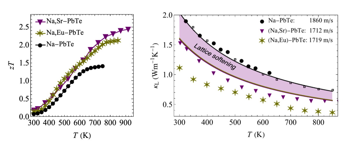
High zT is observed in PbTe with various defects and nanostructures. The low Lattice Thermal Conductivity \(\kappa_\text{L}\) that leads to the high zT results from increased phonon scattering but also lattice softening [23].
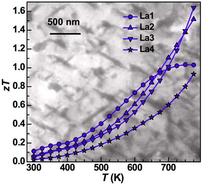
High zT has been observed in several Thermoelectric systems that is attributed to either small [4] or large nanoparticles [5, 10]. We now know that many of the small particles observed in PbTe using a TEM are actually artifacts of the sample preparation [15, 16] and may be indicating the presence of other defects or strain. Much of the improvement in zT has been recently found to be due lattice softening, apparently associated with these defects and strain [23]. The low thermal conductivity is then primarily due to a reduced phonon speed and increased scattering off other phonons rather than phonon scattering off nanoparticle interfaces. Many of the secondary phases likely dissolve into the solid at high temperatures whcih can dope the material (dynamic doping) [25, 26] as well as reduce the thermal diffusivity giving the appearance of a rapid increase in zT at high temperature before the material becomes unmeasurable [27].
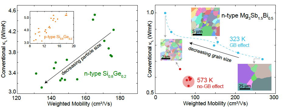
Nanostructuring often results in a decrease in weighted mobility \(\mu_\text{w}\). Ideally for an improvement in zT, there should be a reduction in the Lattice Thermal Conductivity \(\kappa_\text{L}\) as seen in Si-Ge (left). Often the apparent \(\kappa_\text{L}\) actually increases because of Grain Boundary Resistance (right) [17].
It is important, however, that the charge carriers maintain a high weighted mobility to improve zT. Nanostructures and grain boundaries often scatter electrons and produce high interfacial or grain boundary resistance, although it is not commonly pointed out. This reduces the effective weighted mobility and can even give an apparent increase in lattice thermal conductivity (Figure above) [17] which leads to reduced zT.
Thus the critereon for beneficial improvement [20] in thermoelectric performance of a nanomaterial is that the weighted mobility to lattice thermal conductivity ratio must improve:
$$(\mu_\text{w}/\kappa_\text{L})_\text{nano} > (\mu_\text{w}/\kappa_\text{L})_\text{bulk} $$
Thermoelectric Microstructures
The best interfaces and grain boundaries for thermoelectric materials are likely coherent (or semi-coherent), epitaxy-like, low energy interfaces produced slowly. Coherent interfaces such as twin boundaries [18] or semi-coherent low angle grain boundaries made up of dislocations [21, 22] provide an acoustic mismatch that disrupts phonons [24] but may have minimal effect on the electronic structure and are most likely to improve zT. Residual strain from the microstructure also appears to soften materials that slows phonons and leads to more phonon-phonon scattering for higher zT [23]. Methods such as liquid phase sintering [18, 19, 21] might be best suited to produce such a microstructure.
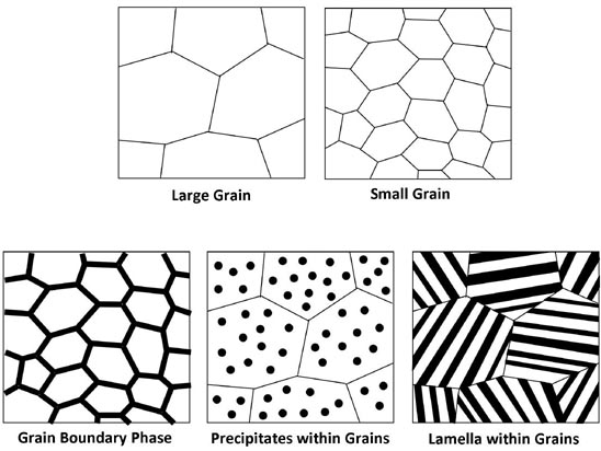
Several methods for producing thermoelectric nanomaterials, or nanometer sized structures in thermoelectric materials have been utilized [2]. Simply by reducing the grain size the lattice thermal conductivity is reduced and significant improvements in zT has been observed [3]. Alternatively nanocomposites, materials with two or more phases can be used to produce a fine microstructure with low lattice thermal conductivity.
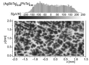
Large inhomogeneaities in Seebeck coefficient observed in a sample that appears to be homogeneous, single phase in SEM and XRD [13].
At macroscopic length scales an inhomogeneous microstructure should not benefit zT. Inhomogeneaities are often at micron or milimeter scale that can be easily missed by TEM microscopy and are better observed with SEM [25]. Sometimes even electron microscopy can miss inhomogeneaities affecting thermoelectric properties. For example, small variations in charge carrier concentration (and type) can dramatically change the Seebeck coefficient from n-type to p-type in a sample that appears to be a homogeneous crystalline material in XRD and SEM [13].
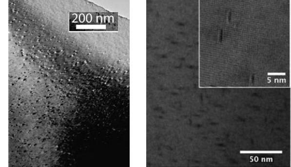
Artifacts produced during sample preparation of PbTe
look like nanoparticles in TEM [15, 16].
Nanometer scale inhomogeneaities are best observed in TEM or APT [14] but could actually be artifacts [15, 16] caused by sample preparation or damage during observation.
Self-Assembly of Composites
There are several methods for forming composite microstructures that utilize phase transformations evident in equilibrium phase diagrams. Such transformations are routinely controlled in metallurgy to strengthen and toughen metals. Nanoprecipitates in aluminum form sol called "GP zones" which impede dislocation movement and dramatically strengthen aluminum. The formation mechanisms in metals are well understood and the microstructures can be controlled to give a variety of morphologies and size scales. Controlled transformation is a means of obtaining 'self-organized' nanostructured thermoelectrics in bulk volumes as an alternative to a layer-by-layer top-down approach.
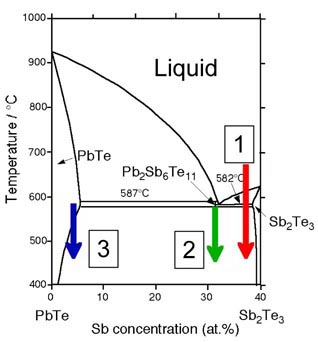
Thermoelectric semiconductor composites can be produced and controlled in much the same manner as metals. Using the PbTe-Sb2Te3 phase diagram for example, three methods for forming composites have been explored.
Solidification
During the Liquid-Solid solidification process (red arrow above) layered crystals of Sb2Te3 are formed until the material cools below the eutectic temperature (582 C). In PbTe rich materials, dendritic microstructure results [6]. By increasing the solidification rate finer microstructure is obtained. Rapid solidification is most successfully employed upon cooling a melt through a eutectic or slightly off-eutectic composition. Feature sizes (interlamellar spacing, secondary dendrite arm spacing, etc.) typically exhibit a power law dependence on an experimental parameter such as cooling rate, solidification time, or growth rate of the solid-liquid interface, with higher cooling rates producing finer microstructures.
With cooling rate of ~10000 K/s using rapid solidification techniques microstructure length scale less than 1 micron can be achieved [7].
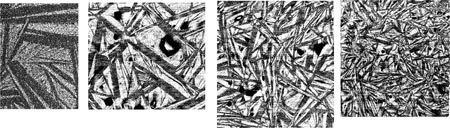
Figure: Control of the size of the microstructure in rapidly cooled
composites of PbTe-Sb2Te3. Shown are the 22 mol% PbTe compositions.
The microstructure length scale is determined by the nucleation and growth kinetics, which in this case is relatively fast because of the rapid diffusion in a liquid.
Alternatively, small microstructures can also be from the direct solidification of eutectic compositions, such as the Ternary Eutectic of Ag-Pb-Te [11] and Ag-Sb-Te [12] shown below.
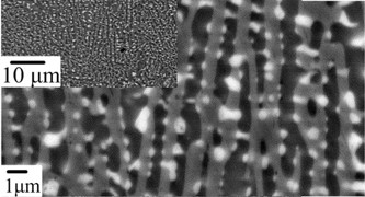
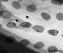
Figure: Nanometer scale Microstructure of Ternary Eutectics formed during solidification. Left: Ag-Pb-Te containing PbTe particles (white) within lamellae composed of Ag3Te5 and Te. Right: Ag2Te nanorods embedded in Ag-Sb-Te matrix.
Eutectoid Decomposition
Phase separation in the solid state can give even finer microstructure because the slower solid-state diffusion. Utilizing the decomposition of metastable Pb2Sb6Te11 into PbTe (light) and Sb2Te3 (dark), a layered (lamellar) microstructure of PbTe and Sb2Te3 is produced when Pb2Sb6Te11 is annealed at a temperature below the stabilization (eutectoid) temperature (mechanism 2, green arrow in phase diagram above). This eutectoid decomposition process and the microstructure formed is very similar to that found in the formation of Pearlite steel. The interlamellar spacing can be controlled by the temperature and time of the decomposition process.
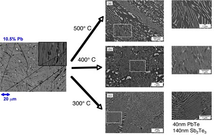
Figure: Microstructure of Pb2Sb6Te11 solid solution transformed
into Sb2Te3 and PbTe rich regions by annealing. The lighter
regions are PbTe, the darker regions Sb2Te3.
Adjacent PbTe and Sb2Te3 lamellae are crystallographically oriented indicating high quality epitaxial interfaces. Average lamellar spacings as small as 180 nm are observed, corresponding to a PbTe layer thickness of 40 nm [8]. These nanoscale multilayers, formed by bulk processing, resemble thin-film superlattices.
Nanostructured thermoelectrics by Precipitation
The solubility in a solid solution is typically temperature dependent. When the temperature drops and the solubility line is crossed (process 3, blue line in the phase diagram above) precipitates will form. The size of the precipitates can be controlled by the cooling rate or annealing temperature if supercooled.
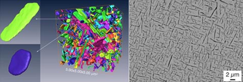
Thin plates of Sb2Te3 precipitate in PbTe with specific crystallographic orientation and habit direction, known as Widmanstätten microstructure [9]. 3-D imaging reveals that both plate like precipitates and elongated ribbon-like precipitates are observed.
Oriented, Epitaxy-like Interfaces
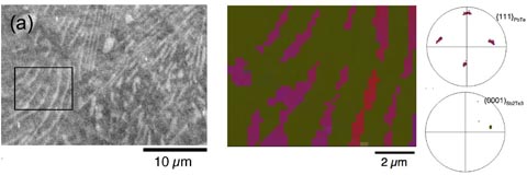
Small, submicron precipitates and lamellae have high surface energy and therefore usually adopt specific orientation relation with the matrix to minimize interfacial energy. In PbTe-Sb2Te3 this corresponds to interfaces along the Te close packed planes: (001) direction in Sb2Te3 and the {111} family of directions in PbTe.
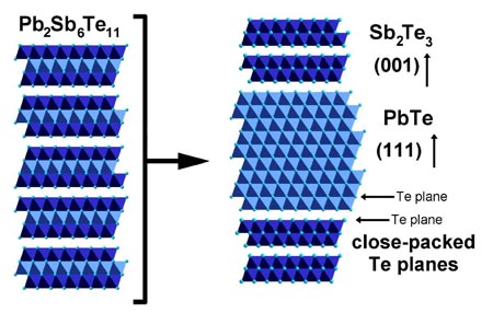
This orientation relationship is observed throughout a grain as seen in the Electron Backscatter Diffraction image where the (001) directions of all the SbTe3 lamellae in a grain (box in panel a below) have the same stereographic projection as the (111) in the adjacent PbTe [8]. In the Widmanstätten precipitates the same orientation relations are found with the habit planes well aligned with the close-packed Te planes.
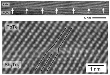
Semicoherent Interfaces
The rather large 6% lattice mismatch is accommodated by periodic dislocations producing a semi-coherent interface as observed in the TEM.
Thermal Conductivity Reduction
It is difficult to show lattice thermal conductivity reduction in the PbTe-Sb2Te3 system because both materials tend to be heavily doped leading to the electronic component dominating the thermal conductivity.
The PbTe matrix phase in the system PbTe-Ag2Te, however, is only lightly doped so that the lattice thermal conductivity can be directly compared as a function of precipitate concentration. Ag2Te precipitates form in PbTe by the same mechanism and with similar size and Widmanstätten morphology as PbTe-Sb2Te3 but have not been as thoroughly characterized.
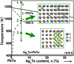
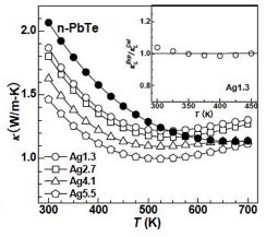
The first 1% of Ag2Te remains dissolved in PbTe at the annealing temperature (500C). Roughly half the Ag substitutes for Pb and the other half enters interstitial positions in PbTe. Both of these defects reduce the lattice thermal conductivity through alloy scattering of phonons.
Higher Ag2Te content produces nanoprecipitates of Ag2Te. In the effective medium theory, such a small volume fraction of secondary phase should have a very small effect on the thermal conductivity even if the interfaces are highly resistive (Kapitza resistance). Yet, the thermal conductivity continues to drop as more Ag2Te particles are added up to 5.5% Ag content. This can be explained by the scattering of long mean free path phonons by the microstructure.
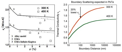
This significant reduction in thermal conductivity may be surprising given that the microstructure is of the order of 100nm while the traditional mean free path of phonons is ~10nm. However there are many long mean free path phonons that carry significant amount of heat. Reducing the mean free path of these phonons to 100nm in PbTe would result in a 20% reduction in lattice thermal conductivity at 300K, similar to that observed in PbTe-Ag2Te.
Improvement in zT
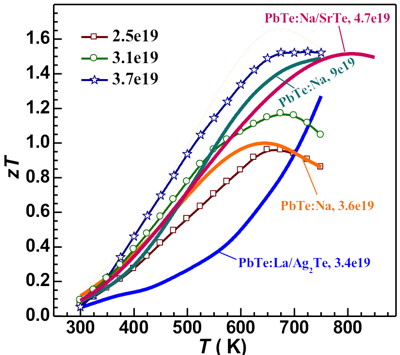
Improved zT requires an appropriate electronic doping. In PbTe-Ag2Te, Na was substituted for some of the Pb adding p-type carriers. The resultant zT is higher, particularly at low temperatures where the reduction in thermal conductivity from the nano composite is most noticeable [10].
References
[1] G. Jeffrey Snyder and Eric S. Toberer "Complex Thermoelectric Materials" Nature Materials 7, 105-114 (2008)
[2] Nicholas A. Heinz, Teruyuki Ikeda, Yanzhong Pei and G. Jeffrey Snyder "Applying quantitative microstructure control in advanced functional composites" Advanced Functional Materials (2014); D.L. Medlin and G.J. Snyder "Interfaces in Bulk Thermoelectric Materials" Current Opinion in Colloid & Interface Science 14, 226 (2009)
[3] Y. Lan, A. J. Minnich, G. Chen, and Z. Ren, Adv. Funct. Mater. 20, 357–376 (2010).
[4] M. G. Kanatizitis, Chem. Mater. 22, 648 (2010)
[5] Y. Pei, J. Lensch-Falk, E. S. Toberer, D. L. Medlin, and G. J. Snyder "High Thermoelectric Performance in PbTe due to Large Nanoscale Ag2Te Precipitates and La Doping" Advanced Functional Materials 21, 241 (2010)
[6] T. Ikeda, S. M. Haile, V. A. Ravi, H. Azizgolshani, F. Gascoin and G. J. Snyder "Solidification processing of alloys in the pseudo-binary PbTe-Sb2Te3 system" Acta Materialia 55, p 1227-1239 (2007)
[7] T. Ikeda, V. A. Ravi, and G. J. Snyder "Microstructure Size Control through Cooling Rate in Thermoelectric PbTe-Sb2Te3 Composites" Met. Mat. Trans. A, 41, p 641 (2010)
[8] T. Ikeda, L. Collins, V. A. Ravi, F. Gascoin, S. M. Haile and G. J. Snyder "Self-Assembled Nanometer Lamellae of Thermoelectric PbTe and Sb2Te3 with Epitaxy-like Interfaces" Chemistry of Materials 19(4) pp 763 - 767 (2007)
[9] T. Ikeda, V. A. Ravi, and G. J. Snyder "Formation of Sb2Te3 Widmanstätten precipitates in thermoelectric PbTe" Acta Materialia 57 p. 666 (2009)
[10] Yanzhong Pei, Nicholas A. Heinz, Aaron D. LaLonde and G. Jeffrey Snyder “Combination of Large Nanostructures and Complex Band Structure for High Performance Thermoelectric Lead Telluride” Energy and Environmental Science 4, 3640 (2011)
[11] Hsin-jay Wu, Wei-jian Foo, Sinn-wen Chen, G. Jeffrey Snyder “Ternary eutectic growth of nanostructured thermoelectric Ag-Pb-Te materials” Applied Physics Letters 101, 023107 (2012)
[12] Hsin-jay Wu, Sinn-wen Chen, Teruyuki Ikeda, G. Jeffery Snyder "Formation of ordered nano-wire microstructures in thermoelectric Pb-Ag-Sb-Te" Acta Materialia 60, 1129–1138 (2012)
[13] Nancy Chen, et al, "Macroscopic Thermoelectric Inhomogeneities in (AgSbTe2)x(PbTe)1-x Materials" Appl. Phys. Lett. Vol 87, p.171903 (2005)
[14] Yuan Yu, et. al, “Revealing nano-chemistry at lattice defects in thermoelectric materials using atom probe tomography” Materials Today 32, 260 (2020)
[15] Xiaomi Zhang et al, "Ion Beam Induced Artifacts in Lead-Based Chalcogenides" Microscopy and Microanalysis 25, 831 (2019)
[16] J.L. Lensch-Falk et al. "Journal of Alloys and Compounds" 504, 37 (2010)
[17] Jimmy J. Kuo et al., “Systematic over-estimation of lattice thermal conductivity in materials with electrically-resistive grain boundaries” Energy & Environmental Science 13, 1250 (2020)
[18] I. Witting et al., “Thermoelectric transport enhancement of Te-rich bismuth antimony telluride through controlled porosity”J. Materiomics 6, 532 (2020)
[19] Y. Pan et al., “Melt-Centrifuged (Bi,Sb)2Te3: Engineering Microstructure toward High Thermoelectric Efficiency” Advanced Materials 30, 1802016 (2018)
[20] Heng Wang, Yanzhong Pei, Aaron D. LaLonde and G. Jeffrey Snyder “The Criteria for Beneficial Disorder in Thermoelectric Solid Solutions” Advanced Functional Materials23, 1586 (2013)
[21] S. I. Kim, et al. “Dense dislocation arrays embedded in grain boundaries for high-performance bulk thermoelectrics” Science, 348, 6230 (2015)
[22] Zhiwei Chen, et al. “Lattice Dislocations Enhancing Thermoelectric PbTe in Addition to Band Convergence” Adv. Mater. 29, 1606768 (2017)
[23] Riley Hanus, et al “Lattice Softening Significantly Reduces Thermal Conductivity and Leads to High Thermoelectric Efficiency” Adv. Mater. 31 1900108 (2019)
[24] R. Hanus, A. Garg, G. J. Snyder, “Phonon diffraction and dimensionality crossover in phonon-interface scattering” Communications Physics, 1, 78 (2018)
[25] Yanzhong Pei, et al. "Self-Tuning the Carrier Concentration of PbTe/Ag2Te Composites with Excess Ag for High Thermoelectric Performance" Advanced Energy Materials 1, 291 (2011)
[26] L. You et al., "Realization of higher thermoelectric performance by dynamic doping of copper in n-type PbTe," Energy & Environmental Science, 12, 3089 (2019)
[27] Agne, et al. “Phase Transformation Contributions to Heat Capacity and Impact on Thermal Diffusivity, Thermal Conductivity, and Thermoelectric Performance” Advanced Materials 31 1902980 (2019)