
Thermoelectric Properties of Materials
Thermoelectric Figure of Merit
The thermoelectric performance (for either power generation or cooling) depends on the efficiency of the thermoelectric material for transforming heat into electricity. The efficiency of a thermoelectric material depends primarily on the thermoelectric materials figure-of-merit, known as \(zT\) [0].
$$zT= \frac{S^2 \sigma}{ \kappa}T\hspace{10 mm} \text{or} \hspace{10 mm} zT=\frac{\alpha ^2}{\rho \kappa}T$$The voltage is produced by the Seebeck coefficient (\(S\) or \(\alpha\)). In addition a low electrical resistivity \(\rho\) (or high electrical conductivity \(\sigma\)) and low thermal conductivity \(\kappa\) is required for high efficiency.
The \(zT\) values of some common materials used commercially, on NASA missions or confirmed in our laboratories is shown below and provide a good baseline for improved materials [0]. Numerous materials with higher \(zT\) have been reported and the field is rapidly advancing, nevertheless one should be aware of stability and measurement issues [13].
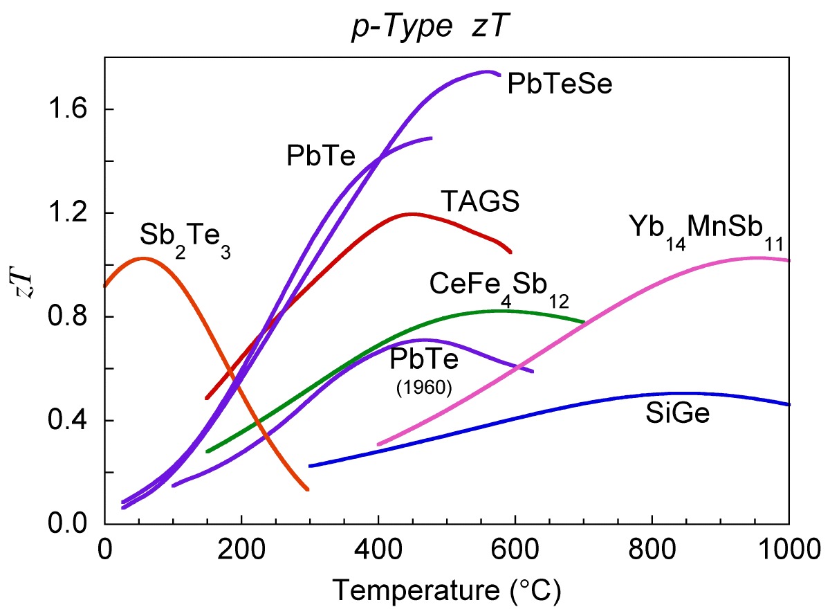
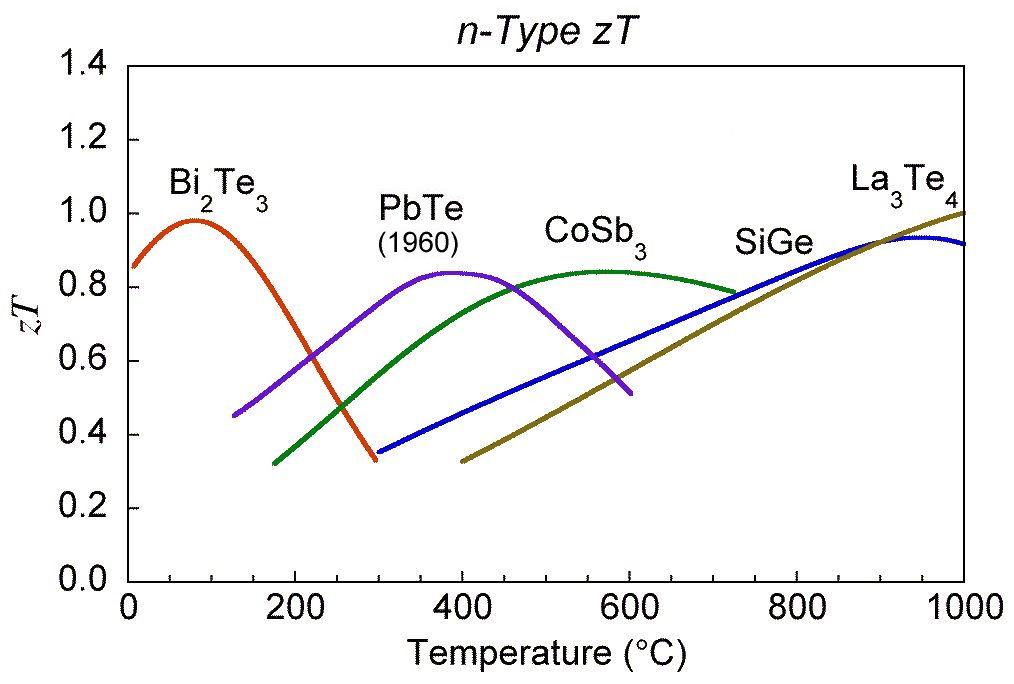
zT for common thermoelectric materials
To achieve sufficient power a TE generator must be used efficiently across a large temperature difference \(\Delta T=T_{\text{h}}-T_{\text{c}}\) and so the material \(zT\) must be high across this temperatre range. The Device \(ZT\) is a weighted average of the TE material \(zT\) that gives the maximum efficiency \(\eta\) across this finite \(\Delta T\) and easily calculated from the material properties \(S\), \(\rho\) and \(\kappa\).
$$\eta=\frac{\Delta T}{T_{\text{h}}}\frac{\sqrt{1+ZT}-1}{\sqrt{1+ZT}+T_{\text{c}}/T_{\text{h}}}$$
Thermoelectric Quality Factor
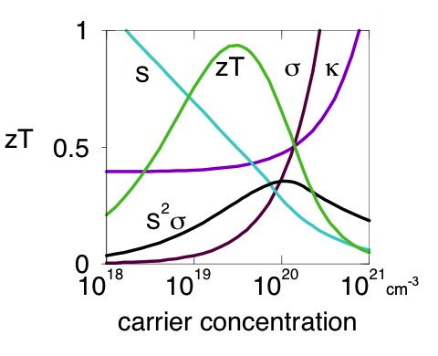
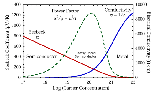
Nearly all good thermoelectric materials are heavily doped semiconductors: semiconductors which have so many free electrons that they have many properties similar to metals. The charge carrier concentration depends on intrinsic defects (such as atom vacancies) as well as extrinsic dopants (impurities). Because all the properties in \(zT\), Seebeck coefficient, electrical resistivity and thermal conductivity depend on charge carrier concentration in a conflicting manner (see figure) achieving high \(zT\) in a material typically requires optimizing the charge carrier concentration.
Thus the search for (or comparison of) good thermoelectric materials is really a search for a material with the highest potential for high \(zT\) presuming it can be optimally doped. This potential high \(zT\) is determined by the thermoelectric quality factor \(B\). The quality factor is determined by the weighted mobility of the electronic charge carriers \(\mu_\text{w}\) and the phonon (or lattice) contribution to the thermal conductivity \(\kappa_\text{L}\).[1, 7]
$$B= \frac{{8\pi k_\mathrm{B}{{\left( {2{m_e}} \right)}^{3/2}}}}{{3e{h^3}}} {\left(k_\mathrm{B} T\right)}^{5/2}\cdot \frac{\mu_\mathrm{w}}{\kappa_\mathrm{L}}=\frac{B_\mathrm{E}T}{\kappa_\mathrm{L}}$$
This shows the quality of a thermoelectric material can be divided into the electronic contribution to the quality factor, \(B_\mathrm{E}\), which is determined by the weighted mobility \(\mu_\mathrm{w}\), and its thermal contribution to the quality factor, which is the lattice thermal conductivity \(\kappa_\mathrm{L}\).[6, 42] These materials properties can be easily evaluated (or at least estimated) from measurements of Seebeck coefficient, electrical conductivity and thermal conductivity, [14], and therefore the potential of a new material can be estimated from a single sample where charge transport is dominated by a single type of charge carrier (electrons or holes).
Improvements in "electronic properties" can be defined as a higher \(B_\mathrm{E}\) (or \(\mu_\mathrm{w}\) at the same temperature), while improved "thermal properties" implies a lower \(\kappa_\mathrm{L}\) for all material changes other than doping. In most good thermoelectric materials phonon scattering of electrons dominates leading to a \(T^{3/2}\) dependence of \(\mu_\mathrm{w}\) which makes \(B_\mathrm{E}\) largely temperature independent. Thus most good thermoelectric materials are reasonably well described with an average value for \(B_\mathrm{E}\) that unlike \(\mu_\mathrm{w}\) is temperature independent [42]. In terms of the transport parameter \(\sigma_{\mathrm{E}_0}\) [14], \(B_\mathrm{E}={\left(\frac{k_\mathrm{B}}{e}\right)}^2\sigma_{\mathrm{E}_0}\).
The overall improvement in thermoelectric materials properties (except for doping) is gauged by the ratio \(\mu_\mathrm{w}/\kappa_\mathrm{L}\). The comparison of \(B_\mathrm{E}\) or \(\mu_\mathrm{w}\) eliminates the need to re-optimize the charge carrier concentration to compare materials and avoids the complication (that is often forgotten) that improved power factor does not necessarily imply higher \(zT\).
Valley degeneracy and deformation potential
The definition of \(\mu_\mathrm{w}\) above is entirely empirical (from measured \(S\) and σ only). Incorporating simple phonon scattering models leads to strategies for improving the quality factor. Because of Fermi's Golden Rule the electron scattering rate τ\(^{-1}\) from phonons should depend on the Density of electron States (DOS) and the electron-phonon interaction strength. Since the interaction is typically less for complex Fermi Surfaces with distant Fermi Surface pockets, the weighted mobility typically scales with effective valley degeneracy \(N_\mathrm{V}\) and the inertial effective mass \(m^*_\mathrm{I}\) used for mobility. This is because the DOS described by the Seebeck mass \(m^*_\mathrm{S}\) can be approximated as \(N_\mathrm{V}\) times the DOS of a single valley described by a band mass \(m^*_\mathrm{b}\).
$$\text{DOS} \propto \left( m^*_\mathrm{S}\right)^{3/2}= N_\mathrm{V}×\left( m^*_\mathrm{b}\right)^{3/2}$$
Then using deformation potential theory for the phonon scattering for intravalley scattering only, the effect of \(m^*_\mathrm{b}\) in \(\mu_\mathrm{w}\) is compensated by increasing τ\(^{-1}\), resulting in
$$B \sim \frac{\mu_\mathrm{w}}{\kappa_\mathrm{L}} \sim \frac{N_\mathrm{V}}{m^*_\mathrm{I} \kappa_\mathrm{L}}$$
This shows better thermoelectric performance can be achieved with a lighter inertial effective mass \(m^*_\mathrm{I}\) (which is related to the band curvature) and/or higher effective valley degeneracy \(N_\mathrm{V}\) [7].
Reducing the phonon or lattice thermal conductivity provides a good opportunity to enhance \(zT\) because it directly appears in the thermoelectric quality factor \(B \sim \frac{\mu_\mathrm{w}}{\kappa_\mathrm{L}}\). This can be done by increasing the phonon scattering by introducing heavy atoms, disorder, large unit cells, and grain boundaries or slowing the phonons so they transport less heat.
Including the effective deformation potential \(\Xi\) and the relevant elastic constant \(C_\mathrm{l}\)
$$B \sim \frac{N^*_\mathrm{V}}{m^*_\mathrm{I} \kappa_\mathrm{L}} \times \frac{C_\mathrm{l}}{\Xi^2}$$
where \(N^*_\mathrm{V}\) is the effective valley degeneracy [7] including the effect of energy offset bands, intervalley scattering and even anisotropy of the Fermi surface [11].
Electronic Properties of Materials
The electronic properties of materials are generally described (as below) using semi-classical terminology that includes the density of charge carriers \(n\), their mobility \(\mu\) and their effective mass \(m^*\) [14]. A more generalized treatment uses the Boltzmann Transport Function Analysis to understand the properties of Complex Electronic Materials.
Electrical Conductivity and Resistivity
The electrical conductivity \(\sigma\) describes the electron current produced when an force that pushes the electrons (such as an electric field) is applied. Often this is measured as electrical resistivity, \(\rho\), the inverse of electrical conductivity, \(\sigma = 1/\rho \), as related to Ohm's law, \(V=IR\). We normally consider just one charge carrying species at a time, but when there are multiple charge carrying species, such as electrons and holes (or electrons in multiple bands), or ions, the total coductivity is the sum of the individual conductivities, combining like resistors in parallel. For example, if just electrons and holes:
$$ \sigma_{total} = \sigma_e + \sigma_h $$
Although resistivity and conductivity are scalar material properties for cubic or isotropic materials, they are tensor properties in general. For most materials (orthorhombic symmetry or greater) simply making sure to measure all properties along the same direction will usually suffice.
Resistivity of a Metal
Electrical resistivities from different dissipating mechanisms typically add like resistors in series and therefore plotting experimental values as resistivities rather than conductivities is usually more helpful in identifying different scattering mechanisms. For example in metals or heavily doped semiconductors such as thermoelectric materials the temperature dependent resistivity often follows the approximate form of a straight line
$$\rho=\rho_0 + \rho_1 T $$where \(\rho_0\) is the resistivity due to electron scattering by defects (impurities, dislocations and grain boundaries) and \(\rho_1 T\) is the resistivity from the atom vibrations (phonon scattering) in a metal. Additional homogeneous scattering mechanisms can be included using Matthiessen's Rule.
Grain boundaries, impurity phases and inhomogeneaities can have profound effects on the measured electrical resistivity but are often ignored as the physical treatment essentially assumes single crystal material. For example a thermally activated resistivity, adding the term \(\frac{\rho_\text{gb}}{d} \exp{\frac{-\Delta E}{k_\text{B} T}}\) to the equation above is often observed from grain boundaries [10] which should increase as the grain size, \(d\) is decreased.
Mobility and Charge Carrier Concentration
In the semi-classical Drude Model, the electrical conductivity is determined by the density of charge carriers \(n\), their drift mobility \(\mu\) and the charge each electron carries \(e\). Here \(n\), \(e\), \(m^*\), \(\tau\) and \(\mu\) are all postitive quantities for both electrons and holes.
$$1/\rho = \sigma = ne\mu$$Mobility typically decreases with effective mass \(m^*\) because heavier objects are harder to move with a force.
$$\mu=\frac{e\tau}{m^*_\text{I}}$$Here \(\tau\) is the scattering time and \(m^*_\text{I}\) is the inertial or conductivity effective mass that in complex materials is different from but related to the density-of-states mass or Seebeck mass \(m^*_\text{S}\) used below [11]. In the Quantum Mechanics based Boltzmann Transport Theory it is the electron group velocity and density-of-states that determines how electrons transport charge. This makes the classical concepts of mobility and effective mass difficult to precisely define and so we will use experimentally based approaches to define them here.
Mathiessen's Rule
When there are multiple scattering mechanisms, Mathiessen's rule is typically used. The scattering rates \((1/\tau)\) are summed for each independent mechanism like resistors in series. $$ \frac{1}{\tau_\text{total}} = \frac{1}{\tau_1} + \frac{1}{\tau_2} + \ldots$$ Mathiessen's rule, particularly when applied to conductivity, implicitly assumes the charge carrier concentration, \(n\) is a constant and homogeneous which may not be the case for grain boundaries and interfaces [10]
Mobility of a Semiconductor
Electron scattering mechanisms are typically identified by their effect on electron mobility. At high temperatures (above 100K) phonon scattering often dominates, and is the only common mechanism that causes a strong decrease in mobility as a function of temperature, \(T^{-1}\) (\(\rho_1\) term above) or faster decrease. For non-degenerate (lightly doped semiconductors) the analytic form typically contains \(T^{-3/2}\) that gradually changes to \(T^{-1}\) for degenerate (heavily doped) semiconductors or metals.
Hall Mobility and Hall Carrier Concentration
The mobility and charge carrier concentration are often estimated using Hall Effect measurements. The Hall carrier concentration (\(n_\text{H}\)) and Hall mobility (\(\mu_\text{H}\)) are derived from the measured Hall Resistance (\(R_\text{H}\)). They are typically within 20% of the true \(n\) and drift \(\mu\) for semiconductors with electronic transport properties dominated by a single type (electron or hole) charge carrier.
$$ n_\text{H} = \frac{1}{eR_\text{H}} $$ $$ \mu_\text{H} = \frac{R_\text{H}}{\rho}$$It is important to remember that when there are both electrons and holes present in a material their Hall effect compensates, decreasing the Hall resistance \(R_\text{H} = \frac{t}{IB}(V_\text{H,h}+V_\text{H,e})\) because their Hall voltages have opposite sign \((V_\text{H,h}>0, V_\text{H,e}<0)\). This will make \(|R_\text{H}|\) smaller than it would be for either charge carrier alone and therefore the measured value of \(|n_\text{H}|\) unrealistically large, larger then either the true \(|n_\text{H,e}|\) or \(|n_\text{H,h}|\) for the electrons or holes.
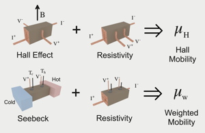
The Hall Mobility is determined from measurements of the Hall Effect and Electrical Resistivity while the Weighted Mobility which gives similar information about charge transport mechanisms can be determined from measurements of the Seebeck Coefficient and Electrical Resistivity [21].
Weighted Mobility
The weighted mobility, easily computed from measurements of the Seebeck coefficient and electrical resistivity can be used like the Hall Mobility to identify charge transport mechanisms by examining the temperature dependence [21]. The weighted mobility is generally described as the drift mobility \(\mu\) weighted by the density-of-states effective mass, while the Hall mobility is approximately the drift mobility.
$$ \mu_\text{w} \sim \mu\left(\frac{m^*}{m_e}\right)^{3/2} \qquad \mu_\text{H} \sim \mu$$
Electron Scattering
The scattering rate is an integral part of transport theory. The scattering time of the semi-classical Drude Model is typically equated with the relaxation time of Boltzmann Transport Theory.
The scattering rate of an electron depends on its velocity, the density of scattering centers and their effective area or scattering cross section [23].
Classical Scattering
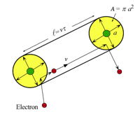
In classical scattering theory the scattering rate, \(1/\tau\), is described by a scattering cross section, which is the effective area, A, the moving particle (with velocity v) sees of a scattering object (where \(n_\text{s}\) is the density of scattering centers). The mean-free-path of the electron is \(\ell = v\tau\).
$$1/\tau = n_\text{s}Av$$
This simple description can be used to justify the physical form of the scattering rate. For example, phonons are atom vibrations where the mean-square-displacement (\(a^2\) in figure above) of atoms is known to increase with temperature as expected from the Equipartition Theorm, \(A=\pi a^2 \sim k_\text{B}T\). All atoms are scatterers so \(n_\text{s}\) is a constant. For a metal, the velocity of electrons does not change much with temperature - that can be described by a high Fermi Velocity. This gives the scattering rate proportional to temperature, explaining the temperature dependent resistivity of a metal, \(\rho_1 T\), described above. For most impurities there is no change in scattering cross section with temperature (vibrations of all atoms is accounted for in the thermal scattering by phonons), only a dependence on the density of impurities through \(n_\text{s}\), explaining the \(\rho_0\) term for a metal.
In a semiconductor, the electrons move appreciably faster if the temperature is increased, approximately following the classical kinetic energy Equipartition Theorm \(½ m v^2 \sim k_\text{B}T\). This gives an additional \(T^{1/2}\) dependence in the scattering rate.
$$1/\tau_{phonon} \propto T \text{(metal)} \qquad 1/\tau_{phonon} \propto T^{3/2} \text{(semiconductor)}$$
This becomes a \(T^{-3/2}\) dependence in the mobility for electron-phonon scattering.
Quantum Mechanical Scattering
In the quantum mechanical description of scattering is easiestly seen using Fermi's Golden Rule. The scattering rate for a particle with energy \(E\) is
$$1/\tau(k) = n_\text{s} g(E) |\langle k |\hat{H'}| k' \rangle|^2 $$
\(n_\text{s}\) is the density of scattering centers. \(\tau(k)\) is the scattering rate of an electron state \(k\) with energy \(E\). \(g(E)\) is the density-of-states that the electron can scatter into. \(\langle k |\hat{H'}| k' \rangle\) is the average matrix element for the purturbation Hamiltonian \(H'\) including the forward scattering term [24]. Here elastic scattering is assumed, where the energy of the electron is unchanged.
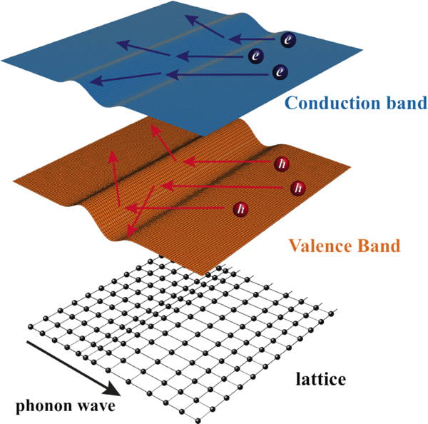
Deformation of a crystal due to a phonon wave, alters the energy of the conduction and valence bands resulting in the scattering of conducting electrons and holes, known as electron-phonon scattering by a deformation potential [12].
Phonon Scattering of Electrons
For example, in deformation potential scattering (deformation of the crystal changes the energy of electrons which scatters transporting electrons) [12]. The mobility parameter is given by $$\mu_0 = \frac{\pi \hbar^4 }{\sqrt{2}}\frac{e}{m^*_I} \frac{C_l}{(m^*_b k_\text{B} T)^{3/2} \Xi^2}$$ [1, 12]. \( m^*_I\) is the inertial effective mass from \(\mu=e\tau/m\); \( (m^*_b)^{3/2}\) is the density-of-states effective mass from the density of electron states; \(\Xi\) is the deformation potential, which is the change in electron energy due to the deformation of the material, calculated from the matrix element \(\langle k |\hat{H'}| k' \rangle\) which also depends on the longitudinal elastic constant \(C_l\) as it relates the force and energy required to deform the material. The \((k_\text{B} T)^{3/2}\) can be understood as the number of phonons (acting as scattering centers \(n_\text{s}\) ) increases with \(k_\text{B} T\) while the speed of scattering electron depends on \((k_\text{B} T)^{1/2}\). Although this scattering is often called Acoustic Phonon Scattering, and the above equation is based on such a theory, Phonon scattering in complex thermoelectric materials, which could be dominated by optical phonons, appears to fit the temperature and energy dependence given above.
Inhomogeneous Materials
Most materials, particularly complex thermoelectric materials, are not single phase crystals. They almost always contain grain boundaries, impurity phases and porosity even if only in trace amounts. The effects of such inhomogeneaities is often ignored in physical models which is not a problem when the effects are small as often is the case in thermoelectric materials where defects are oftened screened. Nevertheless, one should always have an estimate of the approximate volume fraction of phases present and look for common effects of interfaces and grain boundaries on transport properties.
Inhomogenaities occur at many length scales are can be easily misidentified. Common powder X-ray diffraction will often not clearly show impurity phases that are less than 5% by volume. Archimedes density measurement may not detect open porosity. Inhomogeneaities are often at micron or milimeter scale that can be easily missed by TEM microscopy and are better observed with SEM or scanning Seebeck [25]. Nanometer scale inhomogeneaities are best observed in TEM or APT [26] but could actually be artifacts [27, 28] caused by sample preparation or damage during observation.
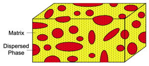
Inhomogeneous material consisting of a random mixture of a Matrix Phase and a Dispersed Phase. The transport properties, such as electrical or thermal conductivity can be estimated using an Effective Medium model requireing only the volume fraction of the dispsersed phase and the properties of each component. Such a model can also be used for porous materials [23].
Effective Medium Models
The easiest estimate for the effect on a material's transport properties is to use an Effective Medium model for an isotropic material such as the Reynolds and Hough rule for mixtures (same as Maxwell Garnett for dielectric constant).
$$ \frac{\sigma_\text{eff}-\sigma_\text{m}}{\sigma_\text{eff}+2 \sigma_\text{m}}=f_\text{d} \frac{\sigma_\text{d}-\sigma_\text{m}}{\sigma_\text{d}+2 \sigma_\text{m}}$$\(\sigma_\text{eff}\) is the effective conductivity of the mixture
\(\sigma_\text{m}\) is the conductivity of the matrix phase
\(\sigma_\text{d}\) is the conductivity of the dispersed phase
\(f_\text{d}\) is the volume fraction of the dispersed phase
Effective Medium models should give results between the ideal case of the materials connected in series or connected in parallel.
Using the magnetic field dependence of the electrical conductivity the properties of the matrix and dispersed phases can be determined [29].
Effective Medium models can also include Interface or grain boundary phases, and effects of anistotropic dispersed phases [30].
Effective Medium \(zT\)
The effective medium model for a thermoelectric shows that the \(zT\) for a composite can never exceed that of its highest component [31]. Thus for a classical mixture of two materials, one containing a high Seebeck coefficient and one containing a high electrical conductivity, the \(zT\) can never be improved. Thus finite size or quantum mechanical effects that effectively alters the mean-free-path (e.g. of phonons) in the high \(zT\) phase is needed to improve \(zT\). The effective power factor can be changed (by altering effective \(A/l\) ratio) but this is not helpful (see power factor discussion below). This classical expectation should be kept in mind when considering the effects of barriers for electron filtering concepts [32, 40].
Porous Materials
For porous materials (containing non-conducting voids) the above Effective Medium Model reduces to
$$ \rho_\text{eff}=\rho_\text{m} \frac{1+½f_\text{d}}{1-f_\text{d}}$$where \(f_\text{d}\) is the volume fraction of the pores. Notice that small volume fractions increase the (electrical or thermal) resistance by 1.5 X the volume fraction of pores: a 99% dense sample should have 1.5% higher resistivity.
When comparing small differences in the properties of porous materials, e.g. looking for nanostructuring effects, one should scale the results with the Effective Medium Model to account for this classically expected increase in electrical and thermal resistance [33].
Grain Boundary Resistance
Grain boundaries and other interfaces are often ignored or treated separately in physics textbooks but can have profound effects on the measured electrical resistivity of polycrystalline materials, particularly at lower temperatures. This is because there is often a thermally activated resistivity, of the form $$\frac{\rho_\text{gb}}{d} \exp{\frac{-\Delta E}{k_\text{B} T}}$$
\(\rho_\text{gb}\) should be an effective, average value for all the interfaces. It has units of an interface resistance, \(\text{Ohm-meter}^2\) or \(\text{Ohm-centimeter}^2\) [\(\Omega\cdot\text{cm}^2\)]. \(d\) is the grain size. \(\Delta E\) is the effective activation energy.
Such a resistance, localized at an interface, can be quite large, such that the apparent mean-free-path might be shorter than an interatomic distance (Ioffe-Regel limit). Clearly the assumptions behind Matthiessen's Rule no longer apply and an inhomogeneous description is needed.
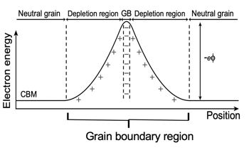
Grain boundary electrical resistance in thermoelectric matreials is likely caused by electrically charged interfaces that trap and/or repel charge carriers [10].
Grain boundary resistance is sometimes considered to be related to Electrical contact resistance where it is thought that shottky barriers produce non-Ohmic contacts. The free charge carrier concentration could also be reduced in the region of the interface by trap states which could justify an inhomogenous region with low conductivity but not unrealistically small mean-free-path. In oxide electroceramics it is known that grain boundaries and other interfaces are often charged providing a barrier to electrical conduction [34].
Thermal boundary or Kapitza Resistance is treated similarly and discussed in the section on thermal properties of materials. The interfacial Seebeck effect, or thermoelectric voltage across a thermal boundary resistance, is much less studied [40].
Regardless of the exact physical model, the phenomenological bricklayer model works well to characterize the electrical [10] and thermal [39] conductivity in polycrystalline thermoelectric materials. A thin resistive grain boundary, uniformly coating conducting grains adds a resistance in series with the grain resistance. The grain boundary resistance should then be inversely proportional to the grain size assuming the grain boundaries have similar properties for large and small grains. The activation energy \(\Delta E\) and \(\rho_\text{gb}\) generally decrease with doping [10] and dielectric constant [35] probably because of charge screening of the barrier. Because many good thermoelectric materials, such as PbTe and Bi₂Te₃ are heavily doped and have high dielectric constant grain boundary effects can be small and overlooked; it enables dense, polycrystalline pellets of material to be analyzed like they were single crystals. However many thermoelectrics with lighter elements, such as Mg₃Sb₂, have significant grain boundary contributions to the resistivity, even at high temperature such that reducing the grain size dramatically improves the \(zT\) [10].
Grain Boundary Complexions
There is a wide variety of grain boundaries in polycrystalline materials that should affect electrical and thermal boundary resistance. We generally believe low energy, low angle grain boundaries or twin boundaries often found in real 'single crystals' should have low boundary resistance. In contrast, high angle grain boundaries have high surface energy and are more likely to accomodate defects that scatter phonons and charged defects that trap and scatter charge carriers. Such interfaces are more likely to attract and collect impurities that will alter (increase or decrease) the grain boundary resistance.
Interfaces in complex materials form low-dimensional equilibrium-like phases called complexions [36]. Each complextion will have different grain boundary resistance. Intrinsic and Extrinsic defects and dopants tend to collect along interface (complexions) and dislocations (Cottrell atmospheres) as have been observed in thermoelectric materials [37]. The thermodynamic complexions should change with chemical potential and therefore should be controlled using Phase Boundary Mapping [38].
The Seebeck Coefficient
In a thermoelectric material there are free electrons or holes which carry both charge and heat. To a first aspproximation, the electrons and holes in a thermoelectric semiconductor behave like a gas of charged particles. If a normal (uncharged) gas is placed in a box within a temperature gradient, where one side is cold and the other is hot, the gas molecules at the hot end will move faster than those at the cold end (in addition to this thermodynamic difference between hot and cold, there can also be a scattering rate difference). The faster hot molecules will diffuse further than the cold molecules and so there will be a net build up of molecules (higher density) at the cold end. The density gradient will drive the molecules to diffuse back to the hot end. In the steady state, the effect of the density gradient will exactly counteract the effect of the temperature gradient so there is no net flow of molecules. If the molecules are charged, the buildup of charge at the cold end will also produce a repulsive electrostatic force (and therefore electric potential) to push the charges back to the hot end.
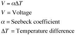
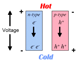
The electromotive force, measured as an electric potential (and electric field \(\vec{E}\) ) produced by a temperature difference is known as the Seebeck effect and the proportionality constant is called the Seebeck coefficient (\(S\) or \(\alpha\)). If the free charges are positive (the material is p-type), positive charge will build up on the cold which will have a positive potential. Similarly, negative free charges (n-type material) will produce a negative potential at the cold end. Here Thermopower refers to the magnitude of the Seebeck coefficient (\(|\alpha |\)).
$$ V = S\Delta T \hspace{10 mm} \text{or} \hspace{10 mm} V = \alpha \Delta T $$ $$ \vec{E} = S\nabla T \hspace{10 mm} \text{or} \hspace{10 mm} \vec{E} = \alpha \nabla T $$
Most of the Seebeck coefficient in electronic systems is related to the equilibrium thermodynamics can be described as the entropy transported per charge transported. Thus \(S\) is often described as related to entropy and carrier concentration \(n\) relative to the density-of-states \(g\) which is characterized by the density of states effective mass \(g\propto (m^*)^{3/2}\). Here we use the Seebeck effective mass \(m^*_\text{S}\) measured by the Seebeck coefficient. There are additional, usually smaller, contributions to the Seebeck coefficient (such as electron scattering) that make this experimental effective \(m^*_\text{S}\) different from other definitions of effective mass. At low temperature (typically less than 100K) and in materials with large phonon thermal conductivity, phonon drag thermopower can be large.
Seebeck Effective Mass
The Seebeck coefficient and charge carrier concentration \(n\) (or Hall \(n_\text{H}\)) can be used to calculate a density-of-state effective mass we call the Seebeck Effective Mass \(m^*_\text{S}\) [11, 14, 41]. Like the Hall mobility and weighted mobility the Seebeck coefficient must be dominated by a single charge carrier type for \(m^*_S\) for easily interpreted. Nevertheless, \(m^*_\text{S}\) can be simply calculated from experimental values of \(S\) and \(n\) (or \(n_\text{H}\)) [41].
$$
\frac{m^*_\text{S}}{m_\text{e}}= 0.924 \left(\frac{300\text{K}}{T}\right) \left(\frac{n_\text{H}}{10^{20}\text{cm}^{-3}}\right)^{2/3} \left[\frac{3\left(\exp\left[\frac{|S|}{k_\mathrm{B} / e}-2\right]-0.17\right)^{2/3}}{1+\exp\left[-5( \frac{|S|}{k_\mathrm{B} / e}-\frac{k_\mathrm{B} / e}{|S|})\right]}+ \frac{\frac{|S|}{k_\mathrm{B} / e}}{1+\exp\left[5( \frac{|S|}{k_\mathrm{B} / e}-\frac{k_\mathrm{B} / e}{|S|})\right]}\right]
$$
Common Forms of the Seebeck Coefficient
The Seebeck coefficient has a number of simple, approximate forms in certain limiting cases - the intermediate cases are described in [1] and [5]. The simple forms can all be related to special cases of the location of the Fermi Level and the transport function \(\sigma_\text{E}\) that also determines electrical resistivity and other electronic transport properties [5]. In systems with a transport edge (band edge or mobility edge) this makes \(\alpha \) a measure of the Fermi Level (\(E_\text{F}\)) relative to the band edge (\(E_\text{B}\)) which is commonly set to zero (replace \(E_\text{F}\) with \(E_\text{F}-E_\text{B}\) in the equations below when \(E_\text{B}≠0\)). The convention when describing only valence bands is to consider the energy of the holes which results in the same equations as electrons for the thermopower (\(|S|\))
Seebeck coefficient of a Metal
In metals or degenerate semiconductors (typically when \(|S| < 100 \mu\text{V/K}\)) where the Fermi level is inside the band (\(E_\text{F}>0\)) the thermopower increases with decreasing charge carrier concentration \(n\) and also increases linearly with temperature \(T\) with a slope proportional to the density of states effective mass \(m^*_S\)
$$|S |= \frac{\pi^2}{3} \frac{k_ \text{B}^2 T}{e} \frac{8m^*_S}{h^2}\left(\frac{\pi}{3n}\right) ^{\frac{2}{3}} \hspace{10 mm} |S |= \frac{\pi^2}{3} \frac{k_ \text{B}^2 T}{e} \frac{1}{E_ \text{F}} $$where \(h\) is Planck's constant. When \(E_ \text{F}\) is in a conduction band (electrons as charge carriers, \(S < 0\) and when \(E_ \text{F}\) is in a valence band (holes as charge carriers, \(S > 0\).
Seebeck coefficient of an Insulator
The thermopower of an insulator often decreases with temperature. In this case the Fermi Level is pinned inside the band gap (\(E_\text{F}< 0\) and is fixed). Here the thermopower of a non-degenerate semiconductor (\(|S| > 200 \mu \text{V/K}\)) is used where the thermopower again depends on the Fermi Level.
$$ |S|= \frac{k_ \text{B}}{e} \left( \frac{-E_ \text{F}}{k_ \text{B}T}+A \right)$$where \(A\approx 2\) depends on the scattering. Again \(S < 0\) for electrons and \(S > 0\) for holes.
Heikes Formula
The Seebeck coefficient of a narrow band system, often used for insulating transition metal and rare earth oxides is given by the Heikes formula.
$$ S = \frac{k_ \text{B}}{e} ln\left( \frac{c}{1-c} \right)$$where \(c\) is the fraction of states in the narrow band that are occupied by electrons. Here the Seebeck coefficient is entirely given by the entropy change due to adding an electron (\(S< 0\) for small \(c\)) that becomes zero for a half filled band ((\(c=\frac{1}{2}\)) and changes sign when \(c>\frac{1}{2}\) when the system is better described by holes rather than electrons.
Weighted Mobility and Power factor
The weighted mobility \({\mu_\text{w}}\) is the best descriptor of the electronic part of the quality factor that makes a good thermoelectric material \(B \sim \frac{\mu_\text{w}}{\kappa_\text{L}}\). Thus any strategy to improve a material for thermoelectric use by reducing \(\kappa_\text{L}\) needs also to consider the effect on \(\mu_\text{w}\).
The weighted mobility can be defined as a simple function of two measured properties, the Seebeck coefficient and the electrical resistivity [21].
$$\mu_\text{w}=331 \frac{\text{cm}^2}{\text{Vs}}\left(\frac{m\Omega\text{cm}}{\rho}\right)\left(\frac{T}{300\text{K}}\right)^{-3/2}\left[\frac{\exp\left[\frac{|S|}{k_\mathrm{B} / e}-2\right]}{1+\exp\left[-5( \frac{|S|}{k_\mathrm{B} / e}-1)\right]}+ \frac{\frac{3}{\pi^2}\frac{|S|}{k_\mathrm{B} / e}}{1+\exp\left[5( \frac{|S|}{k_\mathrm{B} / e}-1)\right]}\right]$$In the simple free electron model, the weighted mobility \(\mu_\text{w}\) is the drift mobility \(\mu\) weighted by the density-of-states \(g\propto \left(m^*\right)^{3/2}\).
$$\mu_\text{w} = \mu\left(\frac{m^*}{m_e}\right)^{3/2}$$
Combining the weighted mobility \(\mu_\text{w}\) as defined above from the Seebeck coefficient and the Hall mobilty for \(\mu\) leads to the definition of \(m^*_S\) the Density of States effective mass derived from Seebeck and Hall measurements.
Power Factor
Historically, \(S^2\sigma\), referred to as the thermoelectric "power factor" has been discussed to evaluate improvements in the electronic properties of thermoelectric materials or when thermal conductivity measurements are unavailable.
Although \(S^2\sigma\), like \(zT\) peaks at a charge carrier concentration between a metal and typical semiconductor, \(S^2\sigma\) does not optimize where \(zT\) does (figure above), overemphasizing more metallic doping concentrations because it ignores the impact of the electronic thermal conductivity \(\kappa_{\text{e}}\) to \(zT\). \(S^2\sigma\) is frequently over analyzed to the point where it is incorrectly concluded that a high \(S^2\sigma\) is preferable even at the expense of lower \(zT\). An optimized thermoelectric design will produce more power when the material is optimized for \(zT\) because it converts the heat flowing through it to electricity most efficiently [8].
The weighted mobility, \({\mu_\text{w}}\) is a better descriptor of the electronic properties for thermoelectric use than \(S^2\sigma\), and with the use of the equation above is easy to calculate from the experimental \(S\) and \(\rho\) (or \(\sigma\)). For example, rather than report peak power factors, a more useful comparison would be to compare \({\mu_\text{w}}\) at a given temperature.
Electronic Contribution to the Thermal Conductivity
Electrons transport heat as well as charge and therefore contribute to the thermal conductivity that reduces \(zT\). To a good approximation, the thermal conductivity of a semiconductor is the sum of the thermal conductivity from the free electrons (or holes) \(\kappa_{\text{e}}\) and the thermal conductivity of the phonons (atomic vibrations) often called the lattice thermal conductivity \(\kappa_{\text{L}}\).
$$ \kappa = \kappa_{\text{e}} + \kappa_{\text{L}}$$
The electronic thermal conductivity derives from the same the transport function \(\sigma_\text{E}\) that also determines the Seebeck and electrical resistivity. For a system with only one type of electron or hole charge carriers (otherwise see bipolar thermal conductivity) \(\kappa_{\text{e}}\) is well approximated with the Wiedemann-Franz law $$\kappa_{\text{e}}=L\sigma T$$ where \(L\) is the Lorenz factor. [Note that some older textbooks use the law differently as if ignoring \(\kappa_{\text{L}}\)]
Like the Seebeck coefficient \(S\), the Lorenz factor \(L\) depends primarily on the location of the Fermi Level (in a single band system) and so a good estimate for \(L\) (at any temperature) is based only on the measured thermopower (\(|S|\)).
$$\frac{L}{10^{-8}\text{W}\Omega \text{K}^{-2}}=1.5+\exp\left(\frac{-|S|}{116\mu \text{V/K}}\right)$$
where \(L\) is measured in \(10^{-8}\text{W}\Omega \text{K}^{-2}\) and \(S\) in \(\mu\text{V}/\text{K}\)[4].
Thus the most common way of reporting phonon thermal conductivity \(\kappa_{\text{L}}\) is to calculate $$\kappa_{\text{L}}=\kappa-L\sigma T$$ where \(\kappa\) is the measured total thermal conductivity and \(L\) is estimated from the measured value of \(|S|\). When \(\kappa_{\text{L}}\) appears to rise at high temperatures due to the bipolar effect \(\kappa-L\sigma T\) is perhaps best refereed to as \(\kappa_{\text{L}}+ \kappa_{\text{b}}\).
Bipolar Effects
When there are significant number of both electrons and holes contributing to charge transport (bipolar charge transport) the thermoelectric properties are greatly affected. This occurs when electrons are excited across the band gap producing minority charge carriers (e.g. holes in an n-type material) in addition to majority charge carriers (e.g. the electrons in an n-type material). Bipolar effects are observed in small band gap materials at high temperature (\(k_\text{B} T \sim E_\text{g}\)) and intrinsic (undoped) semiconductors where (\(n_\text{e} \sim n_\text{h}\)). The equations for two-band (n-type conduction band and p-type valence band) transport given below are special forms of the generalized multi-band result given in [1].
Bipolar Conductivity
The electrical resistivity is least affected because both electrons can holes contribute to the electrical conductivity with the same sign.
$$\sigma = n_\text{h} e|\mu _\text{h}| + n_\text{e} e|\mu _\text{e}|$$
where \(n_\text{h}\) is the density of holes in the valence band and \(n_\text{e}\) is the density of electrons in the conduction band, both positive quantities.
Bipolar Seebeck
The Seebeck coefficient is dramatically affected because the minority charge carriers add a Seebeck voltage of opposite sign as the majority carriers greatly reducing the thermopower \(|S|\). The contribution of each charge carrier to the total Seebeck coefficient is weighted by the electrical conductivity [1].
$$S = \frac{S_\text{h} \sigma _\text{h} + S_\text{e} \sigma _\text{e}}{ \sigma _\text{h} + \sigma _\text{e}}$$
Because \(S_h>0\) but \(S_e<0\) the resultant thermopower will be less when minority charge carriers have significant conductivity.
Bipolar Hall Effect
The Hall voltage, which is also opposite for electrons as holes, is also compensated when both electrons and holes are present making the apparent Hall carrier concentration \(n_{\text{H}} = \frac{1}{eR_{\text{H}}}\) increase much faster than the real majority carrier concentration. The individual contributions are even more strongly weighted by the electrical conductivity (mobility) than is the Seebeck coefficient [1, 9] (note that in this notation \(\mu _\text{h} > 0\) for holes and \(\mu _\text{e} < 0\) for electrons).
$$R_{\text{H}}= \frac{1}{en_{\text{H}}} = \frac{\sigma_\text{h} \mu _\text{h} + \sigma_\text{e} \mu _\text{e}}{ \left(\sigma _\text{h} + \sigma _\text{e}\right)^2}$$
Bipolar Electronic Thermal Conductivity
The thermal conductivity is also affected by the bipolar effect but it is often not noticed because of the lattice contribution. Because there are more electron-hole pairs at high temperature then low temperature, in a temperature gradient there will be an effect of absorbing heat at the hot end by creating electron-hole pairs and releasing heat at the cold end when they recombine.
$$\kappa_{\text{ele}}= L _\text{h}\sigma_{\text{h}}T + L _\text{e}\sigma_{\text{e}}T + \left(S_{\text{h}}- S_{\text{e}} \right)^2 \frac{\sigma_{\text{h}} \sigma_{\text{e}}T}{ \left(\sigma _\text{h} + \sigma _\text{e}\right)}$$
where the last term can be considered the bipolar thermal conductivity that increases exponentially with temperature as \(\exp{\frac{E_\text{g}}{k_\text{B} T}}\)
Thermopower Peak and Band Gap
By having a band gap large enough, n-type and p-type carriers can be separated, and doping will produce only a single carrier type. Thus good thermoelectric materials have band gaps large enough to have only a single carrier type but small enough to sufficiently high doping and high mobility (which leads to high electrical conductivity).
In a semiconductor at high enough temperature electrons will have enough energy to excite across the band gap. When that happens there will be both n-type carriers in the conduction band and p-type carriers in the valence band such that the resultant thermopower will be compensated (reduced) because the two contributions subtract. In a heavily doped semiconductor, where the dopants produce many majority carriers (could be either n-type or p-type) the thermopower will be reduced at high temperature due to the excitation of minority carriers of opposite sign. Although there are fewer minority carriers than majority carriers, they have a larger thermopower. This leads to a peak in the thermopower as a function of temperature.
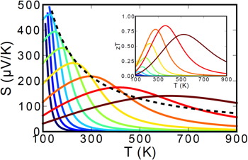
The Figure above shows how the Seebeck coefficient changes when the doping changes from lightly doped (blue) to heavily doped (red).
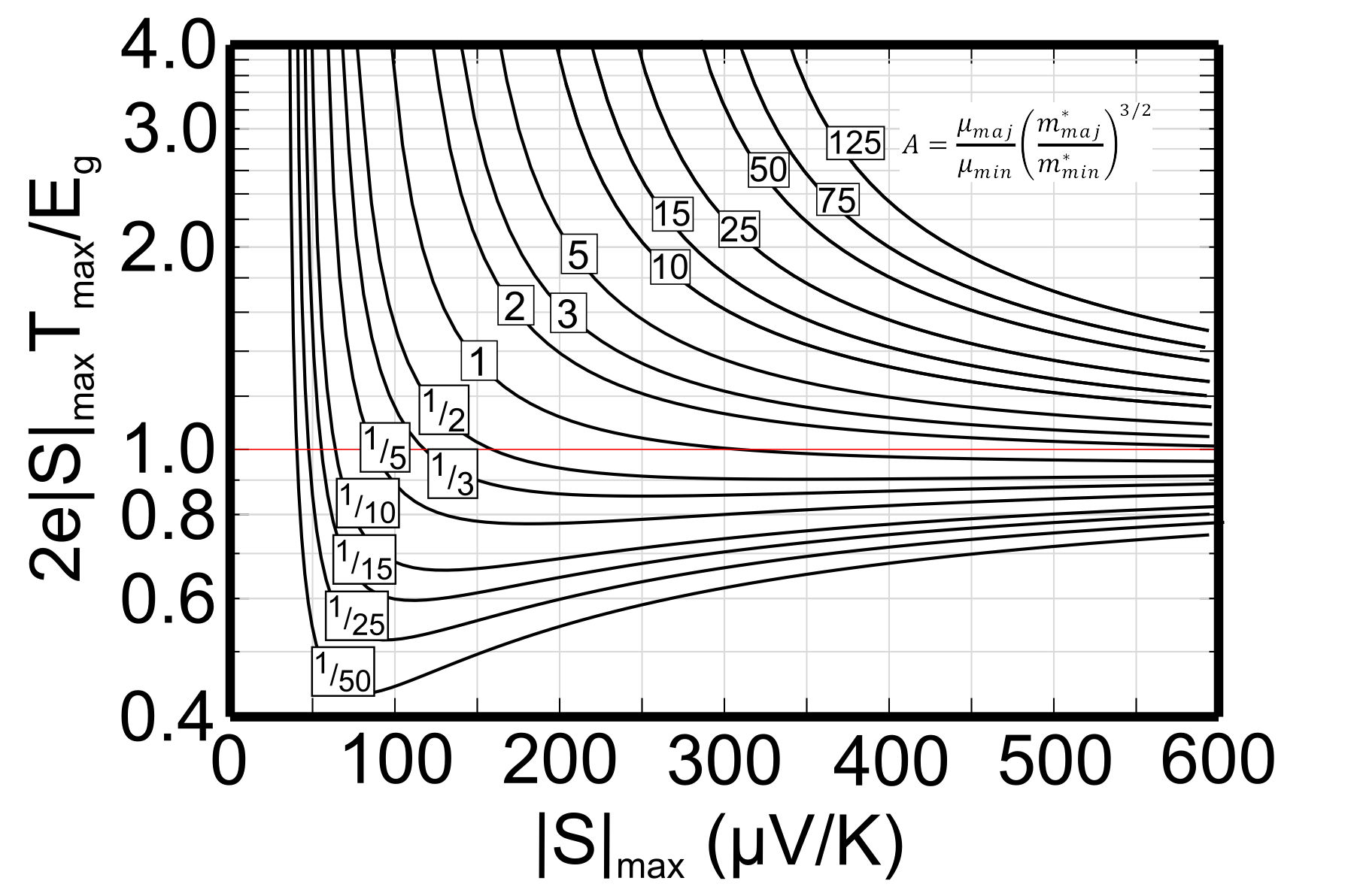
The Temperature at which the thermopower peaks, \(T_{\text{max}}\), and the thermopower of the peak, \(|S_{\text{max}}|\), can be used to estimate the semiconducting band gap, \(E_{\text{g}}\) [3].
$$ E_{\text{g}}=2e |S_{\text{max}}|T_{\text{max}}$$
This equation can be reasonably accurate when both electrons and holes have similar weighted mobility, \(A=\frac{\mu _{\text{w,maj}}}{\mu _{\text{w,min}}}=\frac{\mu _{\text{maj}}}{\mu _{\text{min}}}\left(\frac{m^* _{\text{maj}}}{m^*_{\text{min}}} \right)^{3/2}\) (here \(m^*\) is the DOS mass including valley degeneracy), otherwise the carrier with higher weighted mobility will have a stronger influence and affect the estimation of band gap [3]. The following figure can be used to estimate the error from the Band Gap equation. When the Seebeck peak is greater than 150µV/K this method for measuring Band Gap at high temperature is likely to be accurate.
Thermal Properties of Thermoelectric Materials
Reducing the phonon or lattice thermal conductivity provides a good opportunity to enhance \(zT\) because it directly appears in the thermoelectric quality factor \(B \sim \frac{\mu_\text{w}}{\kappa_\text{L}}\). This can be done by increasing the phonon scattering by introducing heavy atoms, disorder, large unit cells, and grain boundaries or slowing the phonons so they transport less heat.
Callaway Model
Thinking of phonons as classical particles that can transport heat, the thermal conductivity can be considered as comprising the heat capacity, velocity and scattering time for each phonon. Considering the wide spectrum of heat carrying phonons, the Callaway model considers the contribution individually for each frequency \(\omega\).
$$ \kappa = \int c(\omega) v^2_\text{g}(\omega) \tau (\omega) d\omega$$
This is a good way to distinguish the importance of different phonon scattering mechanisms but requires numerical integration. Some simplified analytical forms for \(\kappa\) are discussed below.
Thermal Conductivity from Thermal Diffusivity Measurements
Measurements of thermal diffusivity is now the most common method to experimentally determine thermal conductivity in materials above 200K [13]. The thermal conductivity \(\kappa\) is determined from the measured thermal diffusivity \(D_\text{T}\) and the heat capacity per volume which is the specific heat \(c_\text{P}\) (heat capacity per mass) times density \(\unicode{x00FE}\).
$$\kappa =D_\text{T} c_\text{P} \unicode{x00FE}$$
Heat Capacity
Estimation of the heat capacity of a solid above 200K based on simple physical principles is often more accurate than measurements [13]. Unless there are phase changes in the material, the Dulong-Petit heat capacity of \(3 k_\text{B}\) per atom is usually accurate at high temperatures for the heat capacity at constant volume and to within 10% for the heat capacity at constant pressure for up to a few times the Debye temperature.
\( c_\text{DP}\) is often the best estimate for \(c_\text{P}\) of a new material if the Debye temperature (from elastic properties or speed-of-sound measurements) is not known. Minor compositional changes are easily accounted for by assuming the heat capacity per atom does not change. For example the specific heat capacity per mass can be calculated from the heat capacity per atom equations given here divided by the average atomic mass in the solid \(M_\text{a}\) (see Neumann-Kopp law).
$$ c_\text{DP} = 3 k_\text{B}/M_\text{a}$$
The heat capacity at constant pressure usually increases linearly with temperature above the Debye temperature due to the enthalpy to thermally expand the solid \(9\alpha^2_\text{L}KV_\text{a}T\) where \(V_\text{a}\) is the volume per atom, \(K\) is the Bulk modulus, \(\alpha_\text{L}\) is the coefficient of linear thermal expansion. If \(\alpha_\text{L}\) and \(K\) are known, for example from thermal expansion speed-of-sound measurements, then a good estimate for the heat capacity is [15]
$$ c_\text{P} =\frac{3k_\text{B}}{M_\text{a}}\left[1+\frac{1}{10^4}\frac{T}{\Theta_\text{D}}-\frac{1}{20}\left(\frac{T}{\Theta_\text{D}}\right)^{-2}\right] + \frac{9\alpha^2_\text{L}KT}{\unicode{x00FE}}$$where \(\unicode{x00FE}=M_\text{a}/V_\text{a}\) is the density.
Phase Transformation Heat Capacity
When phase transformations occur on the timescale of measurements the enthalpy of the transformation is included in the heat capacity. For thermal conductivity this timescale is at least the timescale of atomic vibrations and thus significant phase transformation heat capacity has been found in the thermal diffusivity of many materials that are multi-phase or near a phase transformation [17]. This additional heat capacity \(c_\text{p,PT}\) can be related to the enthalpy of transformation \(\Delta H\) and the rate that the phase fraction (order parameter \(\phi\)) changes with temperature which can be estimated with the equilibrium phase diagram [17].
$$c_\text{p,PT}=\frac{\Delta H}{\unicode{x00FE}} \left(\frac{\partial \phi}{\partial T}\right)_\text{p}$$
Debye Model of Phonons
Atomic vibrations in a solid, called phonons, form collective (wave-like), low-energy acoustic modes. Very low energy acoustic modes make acoustic (sound) waves that can be measured as the speed-of-sound \(v_\text{s}\) in a solid. The Debye model approximates all phonon modes to have the same velocity in the dispersion relation of frequency vs. wavevector \( \omega = vk\).
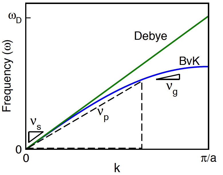
In the Debye model the phase velocity (\(v_\text{p}=\omega/k\)) and group velocity (\(v_\text{g}=d\omega/dk\)) are the same for all phonons. Generally (e.g. Born — von Kármán (BvK) model) this only occurs at \(k\sim0\) where the speed of sound (\(v_\text{s}\)) is measured
The Debye model works surprisingly well considering real solids have longitudinal and transverse modes with different velocities (\(v_\text{l}\) and \(v_\text{t}\)) and have optical as well as acoustic modes that travel with group velocities \(v_\text{g}\) slower than the speed of sound \(v_\text{s}\). Nevertheless, the Debye model sufficiently describes the energy and number of phonon states to provide a good first-order description of atom vibrations in a solid that can be measured with acoustic properties such as the speed of sound.
The number of phonon modes is limited by the number of atoms and this leads to the maximum frequency in the Debye model \(\omega_\text{D}\) that can be described as the Debye Temperature \(\Theta_\text{D}\) and related to the average velocity (here the average speed of sound \(v_\text{s}\)) where \(V_\text{a}\) is the volume per atom.
$$\hbar \omega_\text{D} = k_\text{B}\Theta_\text{D} = \hbar v_\text{s}\left( \frac{6\pi^2}{V_\text{a}}\right)^{1/3}$$
Speed of Sound
The speed of sound from pulse-echo experiments is an easy, accurate method to measure average phonon properties of an isotropic material at room temperature [16]. The average speed of sound \(v_\text{s}\) is an appropriate average of the longitudinal speed of sound \(v_\text{l}\) and transverse speed of sound \(v_\text{t}\).
Often the simple arithmatic mean is used
$$v_\text{s}=\frac{1}{3}\left(v_\text{l}+2 v_\text{t} \right)$$although the average that preserves the phonon density-of-states (probably best for Debye Temperature) is
$$v_s=\left(\frac{1}{3}\left[\frac{1}{v_\text{l}^{3}}+\frac{2}{v_\text{t}^{3}}\right]\right)^{-1/3}$$The speed of sound is directly related to the elastic properties of an isotropic material and so can be estimated from measurements or calculations of the bulk modulus \(K\) and shear modulus \(G\) and density \(\unicode{x00FE}\).
$$v_\text{l}=\sqrt{\frac{K+\frac{4}{3}G}{\unicode{x00FE}}} \hspace{20 mm} v_\text{t}=\sqrt{\frac{G}{\unicode{x00FE}}}$$Note that the speed of sound, phonon velocities, and elastic properties are not isotropic in crystals, even cubic crystals, which makes isotropic polycrystalline materials somewhat easier to work with. \(S\), \(\rho\), and \(\kappa\) are second rank, symmetric tensors which makes them isotropic for cubic crystals.
Minimum Thermal Conductivity
In the extreme scattering limit where the vibrational modes no longer transport heat like propagating waves (propagons or classical phonons) but diffusively and are called diffusons. The minimum thermal conductivity from such heat diffusion can be estimated to be [18]:
$$ \kappa_\text{min} = 0.76 k_\text{B} \frac{ v_\text{s}}{V_\text{a}^{2/3}} $$The Cahill minimum thermal conductivity (high temperature limit) is slightly higher \(1.21 k_\text{B} \frac{ v_\text{s}}{V_\text{a}^{2/3}}\) is a good estimate for glasses.
Umklapp Scattering Thermal Conductivity
In the least scattering limit, phonons are only scattered by other phonons, known as Umklapp scattering. Phonons interact with each other through the anharmonicity where the Grüneisen parameter \(\gamma\) is a good measure. A reasonable estimate for the thermal conductivity of a crystal with no other scattering is [19]
$$ \kappa_\text{u} = C_\text{u} \frac{M_\text{a} v^3_\text{s}}{TV_\text{a}^{2/3}\gamma^2} $$where the constant \(C_\text{u}\sim 0.4/N_\text{c}^{1/3}\) is expected to scale with the number of atoms in the unit cell \(N_\text{c}\) in this way to account only for the acoustic phonon branches [19].
The thermal conductivity of complex materials above the Debye temperature is often of the form \(\kappa=A/T + B\) where the \(A\) is from this umklapp thermal conductivity due to mostly the acoustic branches and \(B\) is the \(\kappa_\text{min}\) minimum or diffuson thermal conductivity from mostly the optical branches close to the value given above. Often \(C_\text{u}\) is better fit to experimental \(A\) value and used as a constant for similar materials.
Grüneisen Parameter
The thermodynamic Grüneisen parameter \(\gamma\) is related to the coefficient of linear thermal expansion \(\alpha_\text{L}\) in an isotropic material.
$$\gamma=\frac{3\alpha_\text{L}K}{c_\text{p}\unicode{x00FE}}$$
Point Defect Scattering of Phonons
The frequency dependence of point defect scattering and umklapp scattering combine fortuitously to give a relatively simple analytical form for the reduction of thermal conductivity due to point defects [22].
$$\frac{\kappa_\text{L}}{\kappa_0} = \frac{\mathrm{tan}^{-1}u}{u} \hspace{20 mm} u^2 = \frac{(6\pi^5V^2_\text{a})^{1/3}}{2 k_\text{B} v_\text{s}}\kappa_0 \Gamma$$Here \(\kappa_0\) is the \(\kappa_\text{L}\) without defects (umklapp \(\kappa_\text{u}\)) and \(\Gamma\) is the average variance from the mass \(\Delta M\) and strain \(\Delta R\) disorder where \(\epsilon\) is a fitting parameter [22]. The benefit to thermoelectrics of point defects must be weighed against the reduction in weighted mobility [20].
$$ \Gamma = \frac{\langle \overline{\Delta M^2} \rangle}{\langle \overline{M} \rangle^2} + \epsilon \frac{\langle \overline{\Delta R^2} \rangle}{\langle \overline{R}\rangle^2}$$
Thermal Boundary - Kapitza Resistance
Interfacial thermal boundary resistance or Kapitza resistance is the thermal analogue of interfacial electrical resistance. Although less commonly studied, it can be similarly measured in different grain size materials and engineered for \(zT\) improvements [39]. The Acoustic Mismatch Model (AMM) explains thermal boundary resistance classically like Snell's law for waves, keeping in mind that acoustic waves have more anisotropy than electromagnetic waves. A microscopic treatment of low angle grain boundaries, made of arrays of dislocations (low energy structure), gives the AMM result in the long wavelength limit and a frequency dependence for phonons with wavelength small enough to interact with the dislocations [24]. The Diffuse Mismatch Model (DMM) is phonomenological and doesnt necessarily capture a classical or quantum limt for phonon scattering at an interface.
Examples of structures with complex anions are shown below in the Skutterudite and Yb14MnSb11 Phases that can be understood with Zintl electron counting rules.
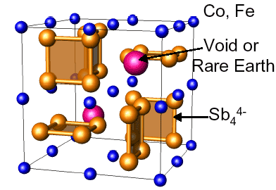
Crystal Structure of Skutterudite
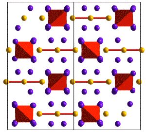
Crystal Structure of Yb14MnSb11
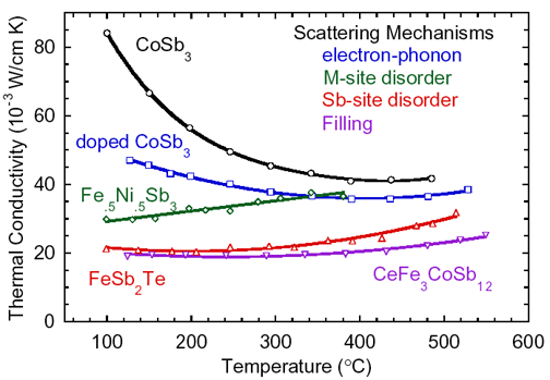
Thermal conductivity decrease in Skutterudites by the
introduction of various scattering mechanisms
Using these principles, a variety of high zT materials have been developed. Many materials have an upper temperature limit of operation, above which the material is unstable. Thus no single material is best for all temperature ranges, so different materials should be selected for different applications based on the temperature of operation. This leads to the use of a segmented thermoelectric generator.
The ideal thermoelectric material is then one which is a "Electron Crystal - Phonon Glass" [1] where high mobility electrons are free to transport charge and heat but the phonons are disrupted at the atomic scale from transporting heat.
[0] G. Jeffrey Snyder and Eric S. Toberer "Complex Thermoelectric Materials" Nature Materials 7, 105-114 (2008).
[1] Andrew F. May, G. Jeffery Snyder "Introduction to Modeling Thermoelectric Transport at High Temperatures" Chapter 11 in Thermoelectrics and its Energy Harvesting Vol 1, edited by D. M. Rowe. CRC Press (2012). Draft Verson .pdf
[2] G. Jeffrey Snyder, Tristan Ursell. "Thermoelectric efficiency and compatibility" Physical Review Letters, Vol 91 p. 148301 (2003)
[3] Zachary M. Gibbs , Hyun-Sik Kim , Heng Wang , and G. Jeffrey Snyder “Band gap estimation from temperature dependent Seebeck measurement—Deviations from the 2e|S|maxTmax relation” Applied Physics Letters 106, 022112 (2015)
[4] Hyun Sik Kim, Zachary Gibbs, Yinglu Tang, Heng Wang, and G. J. Snyder “Characterization of Lorenz number with Seebeck coefficient measurement” APL Materials 3 041506 (2015)
[5] Stephen D. Kang and G. J. Snyder "Charge-Transport Model for Conducting Polymers" Nature Materials 16, 252 (2017)
[6] G. D. Mahan "Good Thermoelectrics" in Solid State Physics Vol. 51 (Eds: H. Ehrenreich ,F. Spaepen ), Academic Press Inc , San Diego 1998 , p. 81.
[7] Yanzhong Pei, Heng Wang and G. Jeffrey Snyder “Band Engineering of Thermoelectric Materials” Advanced Materials 24, 6125 (2012)
[8] L. L. Baranowski, G. J. Snyder , Eric S. Toberer “The Misconception of Maximum Power and Power Factor in Thermoelectrics” J. Applied Physics 115, 126102 (2013)
[9] Tristan Day, Wolfgang Zeier, David Brown, Brent Melot, G. J. Snyder “Determining Conductivity and Mobility Values of Individual Components in Multiphase Composite Cu1.97Ag0.03Se” Applied Physics Letters 105, 172103 (2014)
[10] Jimmy J. Kuo et al., “Grain boundary dominated charge transport in Mg3Sb2-based compounds” Energy & Environmental Science 11, 429 (2018)
[11] Z.M. Gibbs, Francesco Ricci, Guodong Li, Hong Zhu, K. Persson, G. Ceder, Geoffroy Hautier, Anubhav Jain, G.J. Snyder "Effective mass and Fermi surface complexity factor from ab initio band structure calculations" NPJ Computational Materials 3, 8 (2017)
[12] Heng Wang, Yanzhong Pei, Aaron LaLonde and G. Jeffrey Snyder “Weak Electron-Phonon Coupling Contributing to High Thermoelectric Performance in n-Type PbSe” PNAS 109, 9705 (2012)
[13] Kasper A. Borup, Johannes de Boor, Heng Wang, Fivos Drymiotis, Franck Gascoin, Xun Shi, Lidong Chen, Mikhail I. Fedorov, Eckhard Müller, Bo B. Iversen, G. Jeffrey Snyder “Measuring Thermoelectric Transport Properties of Materials” Energy and Environmental Science 8, 423 (2015)
[14] S. Kang and G.J. Snyder "Transport property analysis method for thermoelectric materials: material quality factor and the effective mass model" Chapter VI in
A. Zevalkink, S. D. Kang, G. J. Snyder, E. S. Toberer, et al. "A practical field guide to thermoelectrics: Fundamentals, synthesis, and characterization" Applied Physics Reviews 5, 021303 (2018)
[15] M. T. Agne, G.J. Snyder, et al “Heat Capacity of Mg₃Sb₂, Mg₃Bi₂, and their alloys at high temperature” Materials Today Physics 6, 83 (2018)
[16] Riley Hanus, G. J. Snyder et al “Lattice Softening Significantly Reduces Thermal Conductivity and Leads to High Thermoelectric Efficiency” Advanced Materials (2019)
[17] M. T. Agne, P.W. Voorhees, G.J. Snyder “Phase Transformation Contributions to Heat Capacity and Impact on Thermal Diffusivity, Thermal Conductivity, and Thermoelectric Performance” Advanced Materials (2019)
[18] M. T. Agne, R. Hanus, G. J. Snyder, “Minimum thermal conductivity in the context of diffuson-mediated thermal transport” Energy & Environmental Science 11, 609 (2018)
[19] Eric S. Toberer, Alexandra Zevalkink, and G. Jeffrey Snyder, “Phonon engineering through crystal chemistry” Journal of Materials Chemistry 21, 15843 (2011)(corrected version .pdf)
[20] Heng Wang, Yanzhong Pei, Aaron D. LaLonde and G. Jeffrey Snyder “The Criteria for Beneficial Disorder in Thermoelectric Solid Solutions” Advanced Functional Materials23, 1586 (2013)
[21] Snyder et al, "Weighted Mobility" Advanced Materials, 2001537 (2020)
[22] Gurunathan et al, “Alloy scattering of phonons” Materials Horizons, 7, 1452 (2020)
[23] Kasap, "Electronic Materials and Devices" McGraw Hill, ISBN:0078028183
[24] R. Hanus, A. Garg, G. J. Snyder, “Phonon diffraction and dimensionality crossover in phonon-interface scattering” Communications Physics, 1, 78 (2018)
[25] Nancy Chen, et al, "Macroscopic Thermoelectric Inhomogeneities in (AgSbTe2)x(PbTe)1-x Materials" Appl. Phys. Lett. Vol 87, p.171903 (2005)
[26] Yuan Yu, et. al, “Revealing nano-chemistry at lattice defects in thermoelectric materials using atom probe tomography” Materials Today 32, 260 (2020)
[27] Xiaomi Zhang et al, "Ion Beam Induced Artifacts in Lead-Based Chalcogenides" Microscopy and Microanalysis 25, 831 (2019)
[28] J.L. Lensch-Falk et al. "Journal of Alloys and Compounds" 504, 37 (2010)
[29] Tristan Day, et al. “Determining Conductivity and Mobility Values of Individual Components in Multiphase Composite” Appl Phys. Lett. 105, 172103 (2014)
[30] CeWen Nan, et al. “Effective thermal conductivity of particulate composites with interfacial thermal resistance” Appl Phys. Lett. 81, 6692 (1997)
[31] Bergman, et al. “Thermoelectric properties of a composite medium” J. Appl Phys. 70, 6821 (1991)
[32] Vining, et al. “The B factor in multilayer thermionic refrigeration” J. Appl Phys. 86, 6852 (1999)
[33] I. Witting et al., “Thermoelectric transport enhancement of Te-rich bismuth antimony telluride through controlled porosity”J. Materiomics 6, 532 (2020)
[34] Xin Xu, S. M. Haile et al. “Variability and origins of grain boundary electric potential detected by electron holography and atom-probe tomography” Nat. Mater. (2020)
[35] Tyler Slade, et al. “Understanding the thermally activated charge transport in thermoelectrics: weak dielectric screening leads to grain boundary dominated charge carrier scattering” Energy Environ. Sci. 13, 1509 (2020)
[36] P. Cantwell et al, “Grain boundary complexions” Acta Mater. 62 1 (2014)
[37] Yuan Yu et al, “Revealing nano-chemistry at lattice defects in thermoelectric materials using atom probe tomography” Materials Today 32, 260 (2020)
[38] S. Ohno et al., “Phase Boundary Mapping to Obtain n-type Mg₃Sb₂-Based Thermoelectrics” Joule 2, 141 (2018)
[39] Peng-an Zong, et al. “Skutterudite with Graphene-modified Grain-boundary Complexion Enhances zT Enabling High-efficiency Thermoelectric Device” Energy Environ. Sci. 10, 183 (2017)
[40] Y. Lin et al., “Expression of interfacial Seebeck coefficient through grain boundary engineering with multi-layer graphene nanoplatelets” Energy Environ. Sci. 13, 4114 (2020)
[41] Snyder et al. Advanced Functional Materials (2022)
[42] Zhang et al. Science Advances 6 (2020)
![]()