
Thermoelectrics
Thermoelectric Microdevice
Advances in the microelectronics industry have made it possible to fabricate a multitude of microdevices, such as microprocessors, microsensors, microcontrollers, and microinstruments. These electronic microdevices have significantly reduced power requirements but at the same time require more attention in terms of integrated thermal management and power management and distribution. Micro thermoelectric converters are considered a promising technology approach for meeting some of these new requirements.
Thermoelectric microdevices can convert rejected or waste heat into usable electric power, at moderate (200-500K) temperatures and often with small temperature differentials. They can also be easily integrated and provide effective cooling for devices specific in optoelectronics, such as mid-IR lasers, dense-wavelength-division-multiplexing (DWDM) components and charge-coupled-device (CCD) detectors.
According to scaling factors, the attractive idea behind a thermoelectric microdevice is to increase specific power (W/cm2) by reducing the size of the thermoelectric elements, while maintaining the same aspect ratio of elements in a larger thermoelectric device.


Equally important, miniaturization increases maximum cooling and improves cooling densities. A thermoelectric module generally consists of several n- and p-type leg elements (couples) connected in series electrically and in parallel thermally. A microdevice will enable potentially thousands of these couples to be connected together in a very small area, leading to open circuit voltages of several volts at even modest temperature gradients.
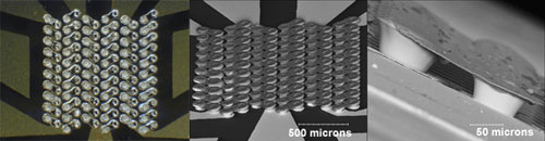
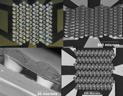
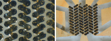
In the Materials and Device Technology Group at JPL, we have developed a unique fabrication method for a thermoelectric microdevice that utilizes standard integrated circuit techniques in combination with electrochemical deposition of compound semiconductors (Bi2Te3/Bi2-xSbxTe3). Our fabrication process is innovative in the sense that we are able to electrochemically micro mold different thermoelectric elements, with the flexibility of adjusting geometry, materials composition or batch scalability. Successive layers of photoresist were patterned and electrochemically filled with compound semiconductor materials or metal interconnects (Au or Ni). A thermoelectric microdevice was built on either glass or an oxidized silicon substrate containing 63 couples (63 n-legs/63 p-legs) at approximately 20 microns in structure height and with a device area close to 1700 mm x 1700 mm. In cooling mode, we evaluated device performance using an IR camera and differential thermal imaging software. We were able to detect a maximum cooling effect of about 2K. In power generation mode, a 75 watt light source was illuminated directly above the device while the current generated was measured. A detailed step-by-step overview of the fabrication process will be given, as well as specifics in testing setups, results and future directions.
Electrochemistry and Materials Properties
Electrochemical deposition (ECD) offers an inexpensive and scalable process. Materials can be varied in composition with deposition rates up to several tens of microns per hour. N-type Bi2Te3 and p-type Bi2-xSbxTe3 compounds were deposited at room temperature at constant potential (EG&G PAR 273A) in a standard three electrode configuration. The working electrode was a metallized oxidized silicon substrate. The cell had a Pt counter electrode and a saturated calomel electrode (SCE) reference. Regions for deposition were defined using a patterned photoresist mask.

Thermoelectric leg elements were deposited from solutions containing dissolved elemental metals with a concentration on the order of 10-3 M in aqueous 1 M HNO3 (pH=0). Solutions containing Sb use chelating agents such as citrate, tartrate or ethylene diamine tetraacetate (EDTA) to allow higher concentrations of the less soluble element at pH 0.
Commercially available gold and nickel bath solutions were used for ECD of bottom base dogbone contacts and top interconnects.
![]()
Photolithography
Photolithographic patterning was performed with a Solitec 3000 HR mask alignment and exposure system (UV power at 750 watts). Two different positive photoresists, Microposit SJR 5740 (Shipley) and Clariant AZ 1518, were used with corresponding Microposit 453 developer and AZ developer. Photoresists were spin coated with a Headway Research, Inc. Photo-Resist Spinner Model 1-PM101DT-R790 and baked on a Cole Parmer 04644 Series Digital Hot plate. Laser printed transparency film and glass masks were designed using Autodesk AutoCAD 2000 Architectural Desktop and printed by CCI Graphics. Successive layers of photoresist were applied as scaffolding for the micro molding of connected thermoelectric couples.
Fabrication Process
The demonstration micro thermoelectric device contains 126 thermoelectric elements 60 µm in diameter and 20 µm tall. Because the resistance of two (Bi, Sb)2Te3 elements is about 0.14 W the metal interconnects must be several µm thick to not contribute overwhelmingly to the device resistance. We use 3 µm thick gold for the bottom interconnects and 3 µm thick nickel for the top, which have resistances of about 0.02 W and 0.05 W respectively.
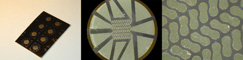
Device fabrication begins with an oxidized silicon substrate (Si/SiO2, 37.5 mm x 50 mm, 0.381 mm thick) substrate. Substrates of this size can accommodate eight microdevices.

We use 400 µm thick oxidized silicon as a substrate because of its high thermal conductivity and compatibility with integrated circuit and MEMS applications. The oxidation layer prevents electrical shorting of the bottom interconnects through the substrate. Onto the substrate is sputtered 0.1 µm Cr, 0.1 µm Au, and then a thicker 3 µm Au layer is deposited by ECD. Using commercial thin positive photoresist (Clariant AZ 1518) and simple transparency film mask, the regions for the bottom interconnects are protected and the surrounding Au is etched (iodine solution). The Cr layer remains and is thick enough to allow further ECD on the isolated Au interconnects.

The thermoelectric layer is formed using a 20 µm thick photoresist mold of positive commercial photoresist (Shipley SJR 5740). By aligning a glass mask, 60 µm diameter holes are patterned on one end of each gold interconnect. The first set of thermoelectric elements (p-type Bi2-xSbxTe3) is electrodeposited to the top of the photoresist.
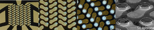
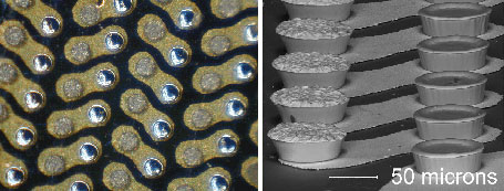

The top interconnects must be formed on a new photoresist layer to build a freestanding bridge between the n-type and p-type elements. First, the thin photoresist layer is selectively removed with a short flood exposure and development to expose the top of the p-type elements. To ensure uniform electrodeposition the entire top surface is sputtered with a very thin layer ( < 0.01 µm) of gold. A fast developing layer of positive photoresist (soft baked SJR5740) is used to form the top interconnect mold. About 3 µm of nickel is grown by ECD into the top interconnect mold. A low stress ECD process is used to ensure the interconnects do not pull off the thermoelectric elements.
Having completed the ECD steps, the photoresist molds and thin gold layer is removed in reverse order. Wet and dry etches and solvents are selected to prevent damage to neighboring structures.
Before operation, samples are annealed in forming gas (7.2% H2 in Ar) at 250oC for 2 hours. Annealing improves mechanical and electrical contact between the thermoelectric elements and the interconnects and also improves the thermoelectric figure of merit of the thermoelectric materials.
The final Cr etch (with KMnO4 solution) electrically isolates the bottom interconnects. All 126 thermoelectric elements are electrically in series, but each of the six rows can be individually addressed with the seven external contacts.
Testing and analysis
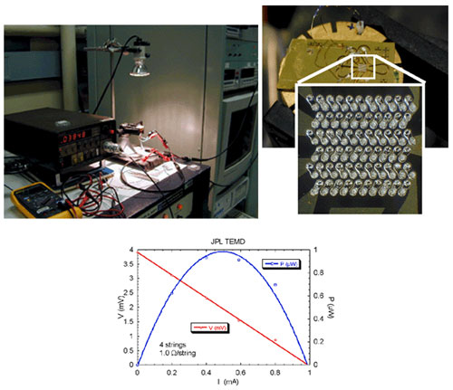
Two isolated gold triangles within each device were used to test for electrical discontinuity, in order to ensure that all the exposed Cr was completely etched away. Typical string resistances range from 2.6W to 5 W and total device resistances range from 12 to 30W (all 6 strings). In fact, string resistances were generally lower after passing current through them. In some cases, as low as 1 ohm per string. Higher resistances were usually attributed to poor or incomplete component contacts and were considered "bad" strings.
In power generation mode, a device was simply mounted on a copper or aluminum block and wired to a computer controlled multimeter and power supply. A 75 watt lamp was illuminated above a glass substrate device, with 4 working strings, as an IV curve was taken and plotted for maximum power. As shown in figure below, power generated was about 1 mW. For both glass and silicon substrate devices, about 1mV/string was produced. This translated to a delta T of approximately 1.25K (V=apnDT, seebeck value obtain from cooling mode). The low power can be attributed to a small DT and non-optimal materials properties (primarily low Seebeck).
In cooling mode, a device on a Si/SiO2 substrate was mounted on a temperature controlled heat sink (thick copper disk on commercial thermoelectric stage) and sealed in a vacuum chamber (~10-6 torr). A PM390 IR camera with temperature resolution of 0.1oC was setup directly above the device. Thermogram Pro (Thermoteknix) software was used to convert 256 levels of luminosity from the camera into temperature. The software included an image subtraction feature used for determining delta temperature changes from device off/on states. Emissivity corrections for the nickel interconnects were performed at around 70oC, and during testing, hotside temperature was held at 90oC (drifted to 82oC during experiment).
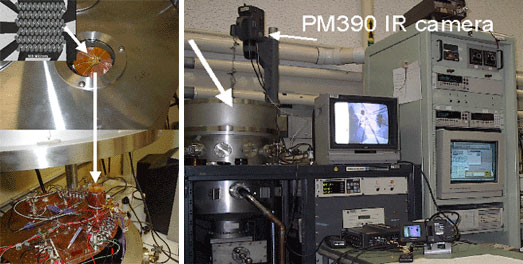

Microdevice Cooling - Turn on microdevice
and pass current to reach maximum delta
T. Observable temperature change through
IR camera and thermal imaging software.
Conclusion
At JPL, we have developed a process to fabricate thermoelectric microdevices using a combination of standard integrated circuit techniques and versatile electrochemical deposition methods. Although, a fabrication process has been established, it is obvious that efforts in materials optimization must be pursued. For example, elements with 1mWcm resistivity were expected to possess a resistance of approximately 0.15W/couple and a Seebeck of 160 mV/K (Sn = -60 mV/K and Sp ~100 mV/K). These values are different from those obtained experimentally.
Clearly, there are many materials and miniaturization issues at such small dimensions, one being contact resistance. Increasing aspect ratios will hopefully alleviate contact resistance concerns and enable a greater DT. More importantly, the optimization of both ECD thermoelectric materials, n-Bi2Te3 and p-Bi2-xSbxTe3, must be investigated further in order to attain near bulk transport properties. Specifically improving p-type resistivity, Seebeck and thermal properties. Lastly, other avenues for device evaluation must also be considered. For instance, such as in cooling mode, it is unclear how device performance is effected by operating at elevated temperatures.
Recent work has been focused on increasing device height (aspect ratio). In order to accomplish and accommodate the demands of various applications, in particular in the optoelectronics industry, our thermoelectric microdevices still need to evolve in design, ECD materials properties, and performance.
Acknowledgments
The authors would like to thank James G. Kulleck for the many scanning electron micrographs and Ronald P. Ruiz for the IR camera work and thermal imaging. In addition, we would like to especially thank Hermes Huang and Dan Daly for their tremendous help and many contributions on this project.
This work is supported by the U.S. Defense Advanced Research Projects Agency, Office of Naval Research and the National Aeronautics and Space Administration
References
G. Jeffrey Snyder, James R. Lim, Chen-Kuo Huang, and Jean-Pierre Fleurial, "Thermoelectric microdevice fabricated by a MEMS-like electrochemical process." Nature Materials, Vol 2, p 528-531 (2003)
J.R. Lim, G.J. Snyder, C.-K. Huang, J.A. Herman, M.A. Ryan and J.-P. Fleurial, "Thermoelectric Microdevice Fabrication Process and Evaluation at the Jet Propulsion Laboratory (JPL)." Twentyfirst International Conference on Thermoelectrics. Proceedings, ICT'02 (IEEE, Long Beach, California, USA, 2002), p. 535.
Fleurial, J.-P., G. J. Snyder, J. Patel, C.-K. Huang, M. A. Ryan, R. Averback, C. Hill and G. Chen. "Solid-state power generation and cooling micro/nanodevices for distributed system architectures" 20th International Conference on Thermoelectrics. P. 24, IEEE (2001)
"Submillimeter-Sized Bi2-xSbxTe3 Thermoelectric Devices " NASA Tech Briefs, Vol. 24, No. 5 (May 2000), NPO-20472
Fleurial, J.-P., A. Borshchevsky, M.A. Ryan, W.M. Phillips, G.J. Snyder, T. Caillat, E.A. Kolawa, J.A. Herman, P. Mueller, and M. Nicolet, "Development of thick-film thermoelectric microcoolers using electrochemical deposition". Materials Research Society Symposium Proceedings, 545 p. 493. (1999).
US Patent 6,288,321